Continue to Site

Welcome to EDAboard.com

Welcome to our site! EDAboard.com is an international Electronics Discussion Forum focused on EDA software, circuits, schematics, books, theory, papers, asic, pld, 8051, DSP, Network, RF, Analog Design, PCB, Service Manuals... and a whole lot more! To participate you need to register. Registration is free. Click here to register now.

[SOLVED] Help pls! n+sd to psub spacing must be <=10um error!

Status
Not open for further replies.

Enorize

Newbie level 4
Joined
Jun 27, 2018
Messages
7
Helped
0
Reputation
0
Reaction score
0
Trophy points
1
Activity points
55
Hey,

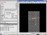
I'm newbie to cadence, and I have final project on cadence a,d exam is in 5 days, and I'm still stuck at this error that prevent me from finishign my final circuit, I use premade transistor layout and capacitors, so when I generate my circuit i got this error, and I don't know hot to solve it at all: n+sd to psub spacing must be <=10um, so please I'm begging you all, help me, I have no one and this is my last ressort.
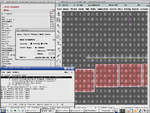
Mandrake Linux-2018-06-25-22-45-05.png

Mandrake Linux-2018-06-25-22-46-36.png

P.s: I'm using cadence virtuoso v5
 

Did you add the bulk terminal?
Or try to place the M1_Psub (Metal 1 and Psub contact) near NMOS.
 

Did you add the bulk terminal?
Or try to place the M1_Psub (Metal 1 and Psub contact) near NMOS.

Ok, I'm newbie to cadence layout, I just did schematic, then i went to: generate from source, I checked circuit with drc,and I got that error, I didn't do anything, and what you mean please by M1_Psub, what's that psub please?
 

Ok, I'm newbie to cadence layout, I just did schematic, then i went to: generate from source, I checked circuit with drc,and I got that error, I didn't do anything, and what you mean please by M1_Psub, what's that psub please?

I guest that you do not have any backgroud knowledge... Everything will be difficult if you do not understand.
I recommend you do some researches about CMOS structure before doing the layout.
Then learn some Cadence Layout tutorials in youtube or somewhere else to get familiar with tool.

About your problem.
In Layout Editor window, press O or click Create -> Via. In Via Definition field, select M1_SUB or something looks like Metal 1 and P substrate.


So in layout, I press O to make a contact and I choose M1_sub, then I place that via where? and connect it to what? sorry I beg you to be patient with me, I studied microelecronic but in my native language, so please be patient with me!:sad:
 

M1_sub contact should be met1, contact, P+, active.

You might look at the actual rule and predecessor logic to
see how the "psub" in question is identified. I have worked
in kits where a "bulk" polygon has to underlie the entire
layout extent (not just a pin-tag on white space). If you
understand what makes "psub" then maybe your answer
will reveal itself.
 

Sorry for beeing late, my computer was broken, I tried to assemble all transistors under 1 bulk, it worked somehow but still I got an error in drc: Multiple stamped connection error!
 

Multiple stamped connection related to bulk usually means that you have several different bulk connections. Use the same bulk connection (possibly a guard ring) for all necessary bulk connections, and connect all these connections by metal to this single bulk connection!
 

Status
Not open for further replies.

Part and Inventory Search

Welcome to EDABoard.com

Sponsor

Back
Top