Continue to Site

Welcome to EDAboard.com

Welcome to our site! EDAboard.com is an international Electronics Discussion Forum focused on EDA software, circuits, schematics, books, theory, papers, asic, pld, 8051, DSP, Network, RF, Analog Design, PCB, Service Manuals... and a whole lot more! To participate you need to register. Registration is free. Click here to register now.

[SOLVED] Problem with Keysight ADS EM simulation

Status
Not open for further replies.

pragash

Advanced Member level 2
Joined
Jul 4, 2005
Messages
512
Helped
64
Reputation
128
Reaction score
59
Trophy points
1,308
Location
Oakland
Activity points
4,940
hi all,
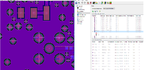
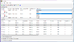
im not able to view my layout which has been imported from Altium via ODB++ format! when i click "3D EM preview", below error appears.

"Pin "L1_1" on mask 1006 is not positioned on the
edge of a slot. Magnetic pins are only supported
on the edge of slots. This setup is invalid."

Please help.
 

"Magnetic pins" in the error message indicates that you have mapped the layer as a "slot plane" instead of a "strip plane".
 
Dear Volker,

Above problem solved. thank you. I got a new problem now.

During EM simulation i got this warning message.

"Port 1 does not have an explicit reference pin, S-parameters may become unphysical at higher frequencies."

i get this warning for every other port in the design. is it ok? or i need to do something?
 

i get this warning for every other port in the design. is it ok? or i need to do something?

Do you have an infinite bottom ground in your stackup that is used for all port ground references?
Can you show your substrate (stackup), and indicate where signal and ground layers are?
 
Do you have an infinite bottom ground in your stackup that is used for all port ground references?
Can you show your substrate (stackup), and indicate where signal and ground layers are?

Dear Volker,
question: Do you have an infinite bottom ground in your stackup that is used for all port ground references?
answer: no, I don't.

question: Can you show your substrate (stackup), and indicate where signal and ground layers are?
answer: im using two layer board stack up with RF on the top layer and DC on the bottom layer. For RF traces, I used CPWG lines. Due to this, the ground plane is on the same layer as RF which is layer L1. Layer L2 is most ground plane but with DC circuits routing in it. Initially I set layer L2 as "slot plane" and that's why the initial error pop up. now I set both to "Strip plane" based on your advice. no error so far but only warning.


my question is;

1) does this warning affects simulation accuracy ? my design range is 0.6GHz to 5.8GHz. this is fundamental frequency of the design and not harmonics.

2) I set cell/wavelength to 80 for above frequency range. is this good enough to provide accurate simulation results which corelates to measurement?
 

1) does this warning affects simulation accuracy ?

Yes, your results might be completely invalid because ...

question: Do you have an infinite bottom ground in your stackup that is used for all port ground references?
answer: no, I don't.

... your ports then lack a valid ground reference. If your return path (ground path) is not an infinite top/bottom ground, then you MUST place explicit pins for the port grounds, and assign them to the (-) terminal of the corresponding ports. Based on the message shown, you didn't do that.

For RF traces, I used CPWG lines. Due to this, the ground plane is on the same layer as RF which is layer L1. Layer L2 is most ground plane but with DC circuits routing in it.

Please show a screenshot that shows pins for signal and ground conductors, and how pins are mapped to port (+) and (-) in the port editor.

2) I set cell/wavelength to 80 for above frequency range. is this good enough to provide accurate simulation results which corelates to measurement?

That sounds like a fine mesh, but it's difficult to answer without seeing the structure. Thick metal and edge mesh settings can have a major influence. But the biggest issue at the moment seems to be your mapping pins to ports (drawn ground plane with no properly assigned port ground references)
 
Dear Volker,
I solved the problem myself.

I realize that all the pins are selected as s-parameter ports including 40 ground pins. I deleted all the pins on the s-parameter ports. I selected only positive (signal) pins and created ports. after that I clicked "set nearest minus pins" and selected all the GND nets.


thank you very much.
my design has 55 ground pins and 127 signal pins. I didn't place the ground pins manually nearby to the signal ports. the ground pins are from the ground pads of the components. is it necessary to place ground pins nearby to each signal ports for reference? does it change the accuracy of the simulation?

- - - Updated - - -

I also manage to convert sheet metal into thick metal as you suggested. for two layer board, its only letting me to do it for bottom copper and not top copper.

- - - Updated - - -

now I have new warnings;

--- WARNING -------------------------------------------------------------------

Layout is electrically large above 3.21 GHz (space wave radiation)

-------------------------------------------------------------------------------
--- WARNING -------------------------------------------------------------------

Substrate is electrically large above 34.5 GHz (surface wave radiation)
RF simulation can be less accurate as it ignores radiation
Consider: - lowering the maximum frequency
- simulating in MW mode

-------------------------------------------------------------------------------
Automatic selection: direct compressed matrix solver
Using multi-threading (8 threads)
Matrix size: 98970 (reduced: 98970)
--- WARNING -------------------------------------------------------------------

The distance between the layout pins for port 2 is electrically large
above 5.02761 GHz, S-parameters may become unphysical.

-------------------------------------------------------------------------------
--- WARNING -------------------------------------------------------------------

The distance between the layout pins for port 9 is electrically large
above 5.20276 GHz, S-parameters may become unphysical.

-------------------------------------------------------------------------------
--- WARNING -------------------------------------------------------------------

The distance between the layout pins for port 10 is electrically large
above 5.20276 GHz, S-parameters may become unphysical.

- - - Updated - - -

Dear Volker,

--- WARNING -------------------------------------------------------------------

The distance between the layout pins for port 2 is electrically large
above 5.02761 GHz, S-parameters may become unphysical.

-------------------------------------------------------------------------------
--- WARNING -------------------------------------------------------------------

The distance between the layout pins for port 9 is electrically large
above 5.20276 GHz, S-parameters may become unphysical.

-------------------------------------------------------------------------------
--- WARNING -------------------------------------------------------------------

The distance between the layout pins for port 10 is electrically large
above 5.20276 GHz, S-parameters may become unphysical.


I manage to solve these problem by moving ground pins closer to the signal pins. now remaining warning is only as below;


--- WARNING -------------------------------------------------------------------

Layout is electrically large above 3.21 GHz (space wave radiation)

-------------------------------------------------------------------------------
--- WARNING -------------------------------------------------------------------

Substrate is electrically large above 34.5 GHz (surface wave radiation)
RF simulation can be less accurate as it ignores radiation
Consider: - lowering the maximum frequency
- simulating in MW mode

-------------------------------------------------------------------------------
 

Attachments

  • ports on ground plane.png
    ports on ground plane.png
    129.8 KB · Views: 529
  • termtype.png
    termtype.png
    36.5 KB · Views: 577
Last edited:

Dear Volker,
my simulation only showing below warning but failed mysteriously. do you understand why its fails?

--- WARNING -------------------------------------------------------------------

Layout healing changed the layout. The actual
highest aggregate snap distance was 9.9694 mil.
Further details have been written to the DRC
report.

-------------------------------------------------------------------------------
Generating mesh at 5.8 GHz...
S-parameter simulation
--- WARNING -------------------------------------------------------------------

Layout is electrically large above 3.21 GHz (space wave radiation)

-------------------------------------------------------------------------------
--- WARNING -------------------------------------------------------------------

Substrate is electrically large above 34.5 GHz (surface wave radiation)
RF simulation can be less accurate as it ignores radiation
Consider: - lowering the maximum frequency
- simulating in MW mode
 

This is the issue that I described above: with finite ground, you need explicit ground pins.

my design has 55 ground pins and 127 signal pins. I didn't place the ground pins manually nearby to the signal ports. the ground pins are from the ground pads of the components. is it necessary to place ground pins nearby to each signal ports for reference? does it change the accuracy of the simulation?

Yes, ground path is equally important as signal path. Any extra length from ground pin in the physically wrong place means simulation error. How much error, that depends on the pin position error vs. wavelength.

I also manage to convert sheet metal into thick metal as you suggested. for two layer board, its only letting me to do it for bottom copper and not top copper.

I don't know what you did, but Momentum lets you define any layer as thick metal (intrude into dielectric above/below instead of thin sheet). I'm using that all the time in RFIC EM work. I recommend using thick metal model if your line/gap with is smaller than 5 * metal thickness, but that number is not a "hard" limit. It also depends on other settings like edge mesh.

thickmet.PNG

--- WARNING -------------------------------------------------------------------
Layout is electrically large above 3.21 GHz (space wave radiation)
-------------------------------------------------------------------------------
--- WARNING -------------------------------------------------------------------
Substrate is electrically large above 34.5 GHz (surface wave radiation)

This warning is critical, expect bad/invalid result. You need to do what the message says: switch Momentum mode from RF to Microwave Mode, to account for possible multimode propagation and radiation.

--- WARNING -------------------------------------------------------------------
The distance between the layout pins for port 2 is electrically large
above 5.02761 GHz, S-parameters may become unphysical.
-------------------------------------------------------------------------------

This warning might be critical, but Momentum starts warning a bit early. Check if your ground pin for the port is placed properly.

I manage to solve these problem by moving ground pins closer to the signal pins. now remaining warning is only as below;

Ok, I'm working through your post step by step. Please see comment above on this warning.

If you think more hands-on support would be useful for reliable results: My company also offers EM methodology consulting and EM training/coaching.
 
This is the issue that I described above: with finite ground, you need explicit ground pins.
yes you did explained in detail and this issue is solved. thank you.

- - - Updated - - -

Yes, ground path is equally important as signal path. Any extra length from ground pin in the physically wrong place means simulation error. How much error, that depends on the pin position error vs. wavelength.

this problem is also sorted. thank you.

- - - Updated - - -

I don't know what you did, but Momentum lets you define any layer as thick metal (intrude into dielectric above/below instead of thin sheet). I'm using that all the time in RFIC EM work. I recommend using thick metal model if your line/gap with is smaller than 5 * metal thickness, but that number is not a "hard" limit. It also depends on other settings like edge mesh.

View attachment 147507
Im designing PCB. I have intrude copper on layer L1 and expand copper at layer L2. I have attached the picture.

top_copper_intrude.png

bottom_copper_expand.png

- - - Updated - - -

when I switch from momentum to microwave mode, all the warning above disappeared with only one more warning which is states as below;

--- WARNING -------------------------------------------------------------------

Layout healing changed the layout. The actual
highest aggregate snap distance was 9.9694 mil.
Further details have been written to the DRC
report.


does it affects the accuracy? if yes, please let me know how to solve it?

- - - Updated - - -

Ok, I'm working through your post step by step. Please see comment above on this warning.

If you think more hands-on support would be useful for reliable results: My company also offers EM methodology consulting and EM training/coaching.

thank you very much for the help. im currently a post graduate student and the university have limited fund for training. I will certainly will contact you soon on my company stuffs as I needs some consulting there.

- - - Updated - - -

--- WARNING -------------------------------------------------------------------

Layout healing changed the layout. The actual
highest aggregate snap distance was 9.9694 mil.
Further details have been written to the DRC
report.


does it affects the accuracy? if yes, please let me know how to solve it?

for this error, do I switch layout healing off?

- - - Updated - - -

I have another basic question. my simulation is EM cosimulation since im simulating the pcb layout and will do circuit simulation with components later. but when I select EM cosimulation, its not simulating. its only simulating in EM simulation/model. why is it so?
 

Im designing PCB. I have intrude copper on layer L1 and expand copper at layer L2. I have attached the picture.

When using expand, the FR4 thickness will be increased and your conductor will be then have FR4 dielectric on the sides, which is not realistic. Have you noticed there is a direction for intrude also? For the bottom layer, you can set metal to intrude into the air layer (or solder stop layer) below.

when I switch from momentum to microwave mode, all the warning above disappeared with only one more warning which is states as below;

As the text says, geometry preprocessing has modified the layout, so that it can be meshed nicely. This preprocessing is configured in emSetup > Options > Preprocessor. There is a "visual aid" button at the top that shows pictures to explain settings.

I don't know what geometry snapped by 9mils, and how much that affects your results. You can check yourself by looking at the mesh. You can also generate a preprocessed layout for visual inspection:

preproc.PNG

- - - Updated - - -

I have another basic question. my simulation is EM cosimulation since im simulating the pcb layout and will do circuit simulation with components later. but when I select EM cosimulation, its not simulating. its only simulating in EM simulation/model. why is it so?

The co-simulation workflow was designed by Agilent/Keysight and I don't like the way they implemented this. You better contact their support to learn about their workflow, and they learn about your difficulty in using it.
 
Last edited:
Dear Volker,
now my simulation shows no error. I unchecked the heal the layout. my design is very compact so I don't want to take chances of inaccurate simulation. thank you very much.
 

Status
Not open for further replies.

Part and Inventory Search

Welcome to EDABoard.com

Sponsor

Back
Top