Continue to Site

Welcome to EDAboard.com

Welcome to our site! EDAboard.com is an international Electronics Discussion Forum focused on EDA software, circuits, schematics, books, theory, papers, asic, pld, 8051, DSP, Network, RF, Analog Design, PCB, Service Manuals... and a whole lot more! To participate you need to register. Registration is free. Click here to register now.

AppCad Values Not Yielding Good Results for CPW

Status
Not open for further replies.

chiques

Full Member level 3
Joined
Nov 21, 2007
Messages
168
Helped
2
Reputation
4
Reaction score
2
Trophy points
1,298
Location
California
Activity points
2,534
Hello Everyone,
I calculated a CPW using Avago’s AppCad. My parameters are:

Εr=3.48
Substrate Thickness=24 mils
Trace Width = 50 mils
Gap=20.5 mils

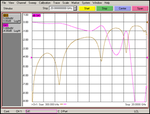
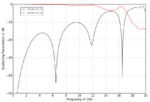
I build this board and it turns out my transmission and reflection begins to deteriorate really bad after 6 GHz.
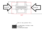
DUT_Connection.png
vna_measurement.png
I also simulated this on a 3D EM simulator. This also shows both my S11 and S21 are poorly performing.
As a sanity check I made the trace thinner (down to 10 mil) and it significantly improved both S11 and S21.
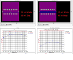
EM_simulation.png
Does anyone have any idea what I’m doing wrong?:?::?::?::?::cry:
 

Does anyone have any idea what I’m doing wrong?

Yes.


This looks like a typical port definition mistake for CPW. It seems that your EM pins on the wide ground conductors are causing electrically large (wide) ports. For physically meaningful results, any port must be electrically small, but your ports span across the complete left (right) edge. This is not correct because it excites uniform currents across the entire width of the port terminals, which is not the correct CPW mode and thus gives wrong results.

Solution: You need to help the EM solver and draw a finite size of the (-) terminals, instead of just placing the pin on the edge. It's difficult to see what tool you used. ADS offers "edge/area" ports for thsi task that I described in my appnote:
https://muehlhaus.com/support/ads-application-notes/edge-area-pins
You can use the edge port described there, and draw a finite length line that specifies each (-) terminals width. I would use a (-) terminal width that is similar to the center conductor width, and starts from the gap.
 
Last edited:

Hello Volker,
I appreciate your response.

Yes.
Your EM pins on the wide ground conductors are causing electrically large (wide) ports. A port must be small, but your port spans across the complete left / right edge. This is not correct and gives wrong results....

I considered my simulation setup being screwed up but I have an actual test board which I've measured on a calibrated VNA using a calibrated E-Cal module. I see this validating my simulation results. An aside from that I can't change the "EM pins on my ground.." on my SMA launch. :roll:

testboard_image.jpg
 

I considered my simulation setup being screwed up

Yes, this looked like typical port definition mistake that I've often seen in my life as an EM support guy.

Your ground connection in the PCB photo also looks terrible - ground current from the SMA would need to go strange ways to get to the "beginning" of the CPW. Ground path routing is just as important as signal path routing. But maybe the connector is nicely soldered on the backside (photo?)

gndpath.jpg
 

..Your ground connection in the PCB photo also looks terrible - ground current from the SMA would need to go strange ways to get to the "beginning" of the CPW. Ground path routing is just as important as signal path routing. But maybe the connector is nicely soldered on the backside (photo?)

View attachment 147400

The bottom view
bottom_view.jpg

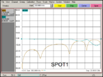
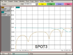
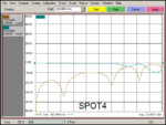
I did think the current flow could have been an issue so I mapped out 4 spots which I would solder then test.
SOLDER_POINTS_0.jpg

I didn't see much of a difference.
Spot1
TRL_THRU_WELD1.png
Spot2
TRL_THRU_WELD12.png
Spot3
TRL_THRU_WELD123.png
Spot4 (all 4 spots soldered)
TRL_THRU_WELD1234.png
 

Ok! As a final test, can you also close the gap on the bottom side (underneath the center conductor) to the connector body?
What is the specified frequency range of your connector? It has much larger pin dimensions than the 18GHz SMA that I used to work with.

If you like, I can also create a 3D EM Model of your layout to double check simulation results. Layout in DXF format would be great, so that we have the exact same layout data.
 

*CORRECTION* from POST #5

That bottom view was from a different sample. Here is the actual bottom view forthis particular sample
bottom_view.jpg

- - - Updated - - -

Ok! As a final test, can you also close the gap on the bottom side (underneath the center conductor) to the connector body?
What is the specified frequency range of your connector? It has much larger pin dimensions than the 18GHz SMA that I used to work with.

If you like, I can also create a 3D EM Model of your layout to double check simulation results. Layout in DXF format would be great, so that we have the exact same layout data.

I will reflow a fillet in these two regions. I'll measure after each solder connection is made and post the results as soon as I have them.
bottom_fillet_regions_0.jpg

The connectors being used are the Johnson/Cinch Part number 142-0701-881 (drawing attached below). They are specified to work up to 18GHz. I also tried 'cutting' the center conductor down (~10mil). That had non-noticeable effect.


A second EM simulation would be great. My *dxf file is attached (zipped BlackMagic.7z).
 

Attachments

  • dr-1420701881.pdf
    442.1 KB · Views: 68
  • BlackMagic.7z
    8 KB · Views: 50

Looking at your connector's data sheet, I suspect that they teaked the layout for that microstrip (!) feed with some magic compensation to achieve good wideband match. For your GCPW, things might be different.

Simulation:

I first checked ADS linecalc results, and noticed that you designed for the quality control (cavity resonator) permittivity value er=3.48 instead of the recommended "circuit design" value er=3.66. This doesn't explain the differences that you observe, but I wanted to bring it to your attention anyway.

gcpw_linecalc.PNG

ro4350b_eps.PNG

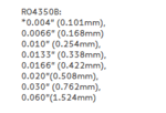
For simulation, I used the thickness that you specified, but looking at the RO4350B data sheet it doesn't seem to be a standard RO4350B thickness value !?

ro4350b_thickness.PNG

I created a model in Empire XPU (3D FDTD EM) using CPW ports, and added vias from top ground to bottom ground.

feed_detail.PNG

To make room for the extra feedlength of the semi-calibrated CPW ports, I extended the line and via fence. The line length between the reference planes ("P1E" and "P2E") is approx. the same as your total PCB length.

model3d.PNG

model2d.PNG

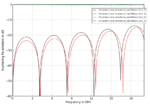
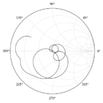
Below are results for both er=3.48 and er=3.66. Return loss is much better than what you observe, with resonable agreement to the 48 Ohm impedance from linecalc.

gcpw_s2p.PNG

Conclusion: I really think you have a discontinuity at the coax - PCB interface that causes poor return loss. In simulation, such a discontinuity can be caused by incorrect port definition. In measurement, I don't trust your coax transition. When I was working in the microwave lab, we used much better (more well defined) transitions at these frequencies.
Given the same line length, simulation and measurement then would show a similar mismatch pattern, for different reasons.

- - - Updated - - -

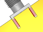
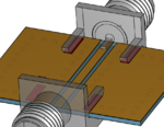
In the meantime, I also created a true 3D model including the SMA, to show what can go wrong. The edge mount SMA has a small airgap (200µm) on the sides and is connected to the PCB using solder (red boxes).

With this, I get rather similar results to your measurements. Note that the line itself was ok, simulation in my previous post. So issue is caused by the connector and how it is connected to ground.

coax1.PNG

coax2.PNG

coax3.PNG

coax4.PNG

Note the narrow gap between SMA and PCB, and note the solder in the ground path.

coax5_gaps.PNG

coax6_gaps.PNG

coax7_gaps.PNG
 
Last edited:

Hey Volker,
I do see a lot of companies using microstrip to characterize their component performance. My guess it’s because it’s easier to implement even though many ‘real world’ applications don’t use it.

Yes, I’ve designed the CPW linecalcs for consistency.

The PCB fab house was able to use prepreg to make this thickness.

Your return loss is surprising. I’m seriously questing my simulation tool now that I see this.

I didn’t think the air gap on the SMA connector would have such an influence!
What happens to the response when zero out the air gap?
 

I do see a lot of companies using microstrip to characterize their component performance. My guess it’s because it’s easier to implement even though many ‘real world’ applications don’t use it.

In 25 years RF/microwave work, I have seen many real world microstrip designs. One reason are the available models when it comes to transmission line components (e.g. filters, but also smaller items like optimum mitered bend models).
Microstrip with side grounds (which you might call coplanar with backside ground) are mostly interconnect in circuits that otherwise consist of lumped elements. I am not aware of any design tool that has complete circuit models for this line type.

Your return loss is surprising. I’m seriously questing my simulation tool now that I see this.

As I wrote in my very first answer, I think your simulated current at the port ground is incorrect. That's a mistake that I see with many EM users doing CPW: they don't realize that placing a pin on a wide edge will cause excitation (current injection) across the entire with of that edge. But the real ground current is near the gap, not equally distributed over the entire edge -> modelling mistake! The solution is to control the port width for the ground pin - that can also be done by adding a small notch.

I didn’t think the air gap on the SMA connector would have such an influence!
What happens to the response when zero out the air gap?

It's not the air gap (only), but the curved flow of current in the ground path. In this configuration, center conductor current can flow "straight on", but ground current can't. This is far from a consistent controlled impedance along the path, with a lot of extra length in the ground path at the SMA-PCB transition -> series L -> local increase in line impedance. Below is a comparison with 200µm and 50µm air gap.

gap_50_200.PNG

The test fixtures for SMA to PCB connections that we used in our lab for measurents were much "better" in terms of not distorting the current flow, and providing a consistent impedance ground path.
**broken link removed**
https://www.anritsu.com/en-GB/components-accessories/products/3680-series
https://www.keycom.co.jp/eproducts/mtf/mtf1/page.html
 
Last edited:

Status
Not open for further replies.

Part and Inventory Search

Welcome to EDABoard.com

Sponsor

Back
Top