Continue to Site

Welcome to EDAboard.com

Welcome to our site! EDAboard.com is an international Electronics Discussion Forum focused on EDA software, circuits, schematics, books, theory, papers, asic, pld, 8051, DSP, Network, RF, Analog Design, PCB, Service Manuals... and a whole lot more! To participate you need to register. Registration is free. Click here to register now.

Offline SMPS with "bent" isolation barrier?

Status
Not open for further replies.
T

treez

Guest
Hello,
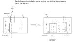
We have an offline SMPS PCB which needs two isolated transformers on it. Both of these transformers have isolated outputs, so therefore both must “straddle” the mains isolation barrier.
The problem is that if the isolation barrier is a straight line running across the PCB, then the two transformers will not fit on the PCB (as shown in the attached diagram).
The PCB is too narrow to fit both transformers on.
Therefore, we wish to make the mains isolation barrier “bent” as also shown in the attached diagram. –This way we can fit the two transformers on the PCB.
However, we worry about noise issues of this unusual shaped isolation barrier. ( noise coupling from primary to secondary side and creating a bigger common mode noise problem). Another point would be where the Y capacitor should go in this “bent” isolation barrier arrangement, so as to best couple noise back to the primary side?
Do you believe that this “bent” isolation barrier is OK?
 

Attachments

  • Two transformers.jpg
    Two transformers.jpg
    78 KB · Views: 139

Hi,

as long as clearance and creapage distance comply with safety rules, there should be no problem.

But I personally don´t like it. Can´t you place it along the long side of the PCB?
Or both transformers back to back with the primary sides?

Klaus
 
  • Like
Reactions: treez

    T

    Points: 2
    Helpful Answer Positive Rating
Put the two transformers on the long side of the pcb. I don't like the bend stuff. Later, it's going to be hard to get a good current return path and cause EMI problem.

The way you do it will waste a lot of pcb space to zig zag the barrier and you end up with less useful pcb space for the other circuits.


Also, you exhausted the choice of transformers available, that you cannot find a narrower transformer? I would look harder.
 
  • Like
Reactions: treez

    T

    Points: 2
    Helpful Answer Positive Rating
Re: Offline SMPS with "bent" isolation barrier?

Put the two transformers on the long side of the pcb. I don't like the bend stuff. Later, it's going to be hard to get a good current return path and cause EMI problem.
Thanks, presumably you mean common mode noise......but then can we not just use more judicious common mode filtering?

- - - Updated - - -

Also, SORRY i dont understand what is meant by putting them on the "long side of the PCB".
 

Re: Offline SMPS with "bent" isolation barrier?

Thanks, presumably you mean common mode noise......but then can we not just use more judicious common mode filtering?

- - - Updated - - -

Also, SORRY i dont understand what is meant by putting them on the "long side of the PCB".

Your drawing of the pcb is rectangle, you put the two transformers along the short side, turn the whole thing 90deg so you put the two transformers along the long side of the rectangle.

I don't mean just common mode noise. There's high current running on the pcb, you have to be careful to make sure the current does not go on a loop with area inside the loop, that will create a lot of EM noise just like a loop antenna. With the bend layout you suggest, the pcb is literally cut up in zig zag form, it's going to be harder to layout to minimize the loop area.

SMPS has a lot of high speed current spikes, if you don't pay attention on the layout and very careful on the ground current return path, you can generate a lot of noise. This topic is in Signal Integrity design.

Isolation barrier.JPG
 
Last edited:
  • Like
Reactions: treez

    T

    Points: 2
    Helpful Answer Positive Rating
Status
Not open for further replies.

Similar threads

Part and Inventory Search

Welcome to EDABoard.com

Sponsor

Back
Top