Continue to Site

Welcome to EDAboard.com

Welcome to our site! EDAboard.com is an international Electronics Discussion Forum focused on EDA software, circuits, schematics, books, theory, papers, asic, pld, 8051, DSP, Network, RF, Analog Design, PCB, Service Manuals... and a whole lot more! To participate you need to register. Registration is free. Click here to register now.

How to deal with large offset voltage in high-power op-amps?

Status
Not open for further replies.

David_

Advanced Member level 2
Joined
Dec 6, 2013
Messages
573
Helped
8
Reputation
16
Reaction score
8
Trophy points
1,308
Location
Sweden
Activity points
12,219
Hello.

I've found this for me very interesting circuit in a paper on Reaserchgate that shows the schematic for a 2mA - 2A AC/DC constant current source made with two OPA544 high-power op-amps, the first is just a unity-gain buffer to supply the required input current to the second which is part of a Howland Current Source, I will post the schematic once I have drawn it in Eagle CAD.

The circuit is incomplete and only feature the actual output stage of what is a system so I have to implement the part of the circuit generating the voltages that should drive the current source which I will do with a microcontroller and a DAC of some kind.

I am in the process of finding out if OPA544 is the best choice since I believe that paper and circuit was made some time ago and there are possibly better choices of op-amp featuring higher GBW(Gain BandWidth product), higher slew-rate, lower offset voltage and so on(if there are other things that might have improved) but even if other power op-amps have become available I will have to deal with between 1mV and 5mV of offset voltage. The only other option I have found from TI at least is the OPA541, there are others such as the OPA2541 but the packages that I can find that in makes it an impossibly expensive part.

The OPA541 features 1mV offset while the OPA544 features 5mV offset, and I find my self hitting a wall thinking about how do I deal with that.
Will that not create a large error in the end in my output setting for the constant current?'
Can I account for it to eliminate it with software?
Can I compensate for it somehow?

Since this is a hobby project sort of thing manual trimming with potentiometers are an acceptable solution even i it isn't the best one, for some reason don't like the idea of trim-pots with a little bit of glue on them to hold them into place, but it worked for the industry before so why not.

But is it really as easy as introducing my own adjustable countering "offset voltage" to one of the op-amp inputs?
Then maybe I could use a high-resolution DAC to make it all done in software, I haven't really gotten to grips with the Howland Current Source and how it actually works but I hope that there are some suitable way of hooking in an ADC to digitize the output current information without adding another current sensing resistor.

Because in order to successfully make the offset adjustment from software I need feedback from an ADC showing the results.

Regards.
 

Hi,

there are two problems with offset:
* A fixed offset. It easily can be cancelled out just by adding any compensating value. This can be done at the analog side or at the digital side.
I´m the friend of doing this at the digital side. It needs no extra parts and is as stable as can be. Digital values won´t drift away.
* And there is offset drift. Much more difficult to compensate, because it will vary with time, with temperature and maybe some other parameters.
Here I recommend to use "low drift" parts and modify the circuit to get low drift (if possible).
Additionally you may include an automatic "offset correction routine" in your software.

Offset correction routine.
* disconnect load
* slowly run a digital ramp form -5mV to +5mV (referenced to the OPAMP input. You may choose any other suitable values)
* check output voltage of your current source with a comparator, (or circuit with a bjt...)
* safe the ramp value when the output jumps frm one rail to the other
* do the same in the opposite ramp direction.
* use the average of both values as your offset compensation value (save the value in the EEPROM)

Mind:
The output of an unlaoded current source will "jump" from one rail to the other at the zero_current border. Thus you don´t need an ADC, just a HIGH/LOW dectection is sufficient.

Klaus
 
  • Like
Reactions: David_

    David_

    Points: 2
    Helpful Answer Positive Rating
Years ago, I saw a circuit where the power opamp stage's offset was servo'ed out with the help of low offset opamp. Basically the analog counterpart of the technique Klaus described.
But being analog in nature, it is complex.

Therefore use the digital technique that Klaus recommends.
 

One key question is, what does 1mV or 5mV of Vio do
to circuit operation? Just a bit of "zero error", or a big
one?

1mV on a 1V input, probably not a biggie. But if your
control input range was only 10mV, yeah, you'd care.

One answer is then to make sure that your control
voltage uses all practical input common mode range,
take your gain early and with higher quality op amps.

If the HPOA input offset looks to be fixed (over time,
temp, supply, ...) then, as you seem to want to use a
uC, there's the possibility of a "cal-map" where you use
after-the-fact accuracy/linearity test data to create a
"right answer transform" table between the figured
target code, and the DAC input, to get the proper output.
 

As others mentioned it’s likely you can address your problems by adding low offset low-power amplifiers either to pre amplify your signals or to implement an outer feedback loop to correct offset. There are many precision opamps and “zero-drift parts between 1 and 10 MHz. Splitting gain between multiple stages may also provide system bandwidth improvements.
 

The OPA544 and OPA541 have some desirable features but I think I will go for the OPA564, it has only a +-12V supply capability(the original design uses a OPA544 and +-35V) but it has far higher bandwidth(full power bandwidth of 1,3MHz at gain = +2, OPA541 have a full power bandwidth in the lower kHz range) but the OPA564 features only 1,5A(1,5A @ 20Vpp output with +-12V supplies) so maybe I'd like to parallel two of those.
As far as offset is concerned the OPA564 has the following:

OFFSET VOLTAGE(VCM = 0V):
Input Offset Voltage(VOS): typ ±2mV, max ±20mV
vs Temperature(dVOS/dT): ±10µV/°C
vs Power Supply(PSRR): typ 10µV/V, max 150µV/V

INPUT BIAS CURRENT(VCM = 0V):
Input Bias Current(IB): typ 10pA, max 100pA
vs Temperature see figure in datasheet...
Input Offset Current(IOS): typ 10pA, max 100pA

Common-Mode Voltage Range(Linear Operation): (V-) to (V+)-3V
CMRR min 70dB, typ 80dB

Slew Rate(G = 1, 10V step): 40V/µs
THD+N(f = 1kHz, RLOAD = 5Ω , G = +1, VOUT = 5VP): 0,003%

I very much like the idea Klaus wrote about, I have been thinking about how to come up with a triangle/ramp waveform with mV's of peak-to-peak amplitude but thus far all I have thinking about is RC generated waveforms and the basics of how analog PWM modulation works which I am not sure will be of much use.

But so that I am sure I understand, the other idea others have been talking about, could that be called a "composite amplifier"?

Which I have seen examples of where they used a amplifier with high DC accuracy to enhance a high-bandwidth amplifier, I don't understand how to combine two other op-amps like that but this might be a good opportunity to learn more about that?

If the 2nd idea is a composite amplifier then I am leaning towards that, but in any case I have great use for the idea from Klaus in a couple of other projects, that idea will be quite fun to implement I think.

If I took the route of using another op-amp to compensate the offset, then there could be other benefits also I presume?

- - - Updated - - -

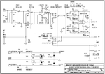
This is the original schematic, published by:
Nandkishor Ghodke*, S. N. Kane#, S. S. Khinchi# and Ajay Gupta*

*UGC-DAE Consortium for Scientific Research (formerly known as IUC-DAEF)
University Campus, Khandwa Road, INDORE – 452 001 (MP), INDIA

#School of Physics, Devi Ahilya University, Khandwa Road Campus, Indore

AC & DC CONSTANT CURRENT DRIVER FOR INDUCTIVE LOAD (2mA TO 2A)_004.jpg
(the first time I loaded this image in the actual post it took something like 25 seconds to load)

I haven't drawn my own schematic yet because I am still deciding about the op-amp and I haven't yet decided upon how to implement the dual 3PDT switches(I think that's right) and the two dual DPST switches.
I will probably go with ordinary mechanical switches for the 3PDT's and relays for the DPST's, but I am considering alternatives to make the thing entirely digital in it's user interface, but I wouldn't mind a couple of nice mechanical switches but I would then also want indicating LED's for which state there in which demands switches with 3 individual switches in each so the third can switch LED's.

If I am not mistaken the buffer op-amp would need to be able to supply at most 200mA which would make it very expensive to use another power op-amp for that buffer unless I would have a dual power op-amp and only needed one of them for the output amplifier.
 
Last edited:

Hi,

(the first time I loaded this image in the actual post it took something like 25 seconds to load)
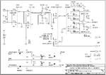
It seems your picture is a low resolution B/W one, which is artifically stretched to higher resolution.

Best is to show to optimize the original one.
But even a bit of optimisation on your uploaded picture gives 1/10 of file size while it still keeps good quality.
ccs5b.png
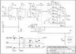
further compression gives 1/50 of file size.
CCS3B.png

Klaus
 

Yeah my quick comments would be to use a low power amplifier for the buffer and consider moving the gain in there. This gives the power amp bigger signals so as to minimize the offset proportionally.

An example composite scheme would be to move the buffer amp so it’s a differential shunt amplifier measuring the current and put the selectable gain there. Now use its output as the feedback for the power amp stage. This feedback signal size can be maximized so it uses much of your available supply range and this minimizes Power amp offset impact. If needed one more amp could scale the input to this range.
 

Status
Not open for further replies.

Similar threads

Part and Inventory Search

Welcome to EDABoard.com

Sponsor

Back
Top