Continue to Site

Welcome to EDAboard.com

Welcome to our site! EDAboard.com is an international Electronics Discussion Forum focused on EDA software, circuits, schematics, books, theory, papers, asic, pld, 8051, DSP, Network, RF, Analog Design, PCB, Service Manuals... and a whole lot more! To participate you need to register. Registration is free. Click here to register now.

[HSpice] Invertor Simulation Problem

Status
Not open for further replies.

EEPuppyPuppy

Junior Member level 3
Joined
Jun 14, 2018
Messages
26
Helped
0
Reputation
0
Reaction score
0
Trophy points
1
Activity points
343
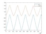
I am trying to simulate an invertor by using this model. However, the output is very wired like the plot below.
untitled.jpg
It does not show the invertor property at all. Also, I have no idea that why the output can even go above the voltage supply.
Could anyone help me? Thank you so much.

Code:
*Single invertor circuit
.LIB '/home/icsrl/TECHNOLOGY/FROM_MOSIS/TSMC/65nm/PDK/CRN65GP/models/hspice/crn65gplus_2d5_lk_v1d0.l' TT

vdd 3 0 DC 1V
vin 1 0 PULSE (0 1 0n 1n 1n 0.1n 2.2n)

*Schimitt trigger circuit
mp1 2 1 3 3 pch L=15u W=60u  
mn1 2 1 0 0 nch L=15u W=15u

cout 2 0 0.1pf

.TRAN 0.01ns 10ns
.option post=1 
.END
 
Last edited:

To invert a signal, the P device must be uppermost. The N device must be at bottom.
Your plot looks as though their positions are reversed, so that they act like emitter followers.
 

To invert a signal, the P device must be uppermost. The N device must be at bottom.
Your plot looks as though their positions are reversed, so that they act like emitter followers.

Thanks for your response. The PMOS is actually at the top which connected to Vdd and the NMOS is at bottom connected to the ground.
 

Status
Not open for further replies.

Part and Inventory Search

Welcome to EDABoard.com

Sponsor

Back
Top