d123
Advanced Member level 5
Hi,
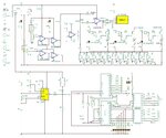
The circuit is an analog electronic load/"electronic load".
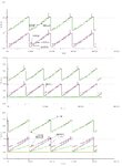
It cycles through 10-step 100 ms (10 ms per step) cycles of: 1) 1mA to 10mA, or 2) 10mA to 100mA, or 3) 100mA to 1A.
At step 1 of 1) and 2) the current at the point of interest is not 1mA or 10mA but ~300uA or ~3mA, the c) 1A version is correct at step 1: 100mA. In 1) and 2), all other steps are correct (2mA upwards and 20mA upwards).
The reference and feedback voltages into U2 are correct during the cycle on 1), 2), and 3) AFAIK. U2 output voltage not included, hope it wasn't necessary - anyway, I just wanted an idea of what no doubt obvious flaw/error of electrical understanding of mine the circuit has that I'm not seeing/haven't experienced before making circuits.
If the problem is not inaccuracy related, is the cause maybe a drop from 2V down to an accurate 200mV (and with no ground bouncy behaviour) is asking too much? Is perhaps the U31 NMOS - or another device in the chain - turning off too slowly? If none of those suggestions, what are possible/typical causes for this symptom?
I'm asking you here because (apart from trying many things to remove this glitch, e.g. adding an eleventh step to provide deadtime after step 10 for an unsuccessful auto-zero attempt) it looks less like a problem specific to a specific circuit and more like one that maybe more experienced eyes will have seen in some shape or another and be able to have a fair guess from the information provided in the pdf.
The pdf includes the schematic (again), the signal path drawn (confusingly, attempting to make it easy to "read"...) on the schematic during step 1 high, and the relevant current and reference voltage waveforms for each shunt resistor (2R, 20R, 200R).
Thanks.


View attachment electronic load version 1 e.pdf
- - - Updated - - -
Hi,
Famous last words... I ran simulations for the op amp and NMOS signals and wonder what may be interpreted from them, if anything at all.
Is the NMOS not being turned on enough? I have become a minor expert in this ...skill asset by now of misjudging VGS min for anything useful.
If so, is there really any reason not to replace it with an equivalent PMOS? How else could I resolve this problem? I will give 1 degrading point out of malice to the person who uses the word bootstrap or close cousins in a reply, by the way.

Any guidance in a vaguely correct direction much appreciated - I've been going around in this circle on this part of the circuit for a week now and I feel tired, help.
Thanks.
The circuit is an analog electronic load/"electronic load".
It cycles through 10-step 100 ms (10 ms per step) cycles of: 1) 1mA to 10mA, or 2) 10mA to 100mA, or 3) 100mA to 1A.
At step 1 of 1) and 2) the current at the point of interest is not 1mA or 10mA but ~300uA or ~3mA, the c) 1A version is correct at step 1: 100mA. In 1) and 2), all other steps are correct (2mA upwards and 20mA upwards).
The reference and feedback voltages into U2 are correct during the cycle on 1), 2), and 3) AFAIK. U2 output voltage not included, hope it wasn't necessary - anyway, I just wanted an idea of what no doubt obvious flaw/error of electrical understanding of mine the circuit has that I'm not seeing/haven't experienced before making circuits.
If the problem is not inaccuracy related, is the cause maybe a drop from 2V down to an accurate 200mV (and with no ground bouncy behaviour) is asking too much? Is perhaps the U31 NMOS - or another device in the chain - turning off too slowly? If none of those suggestions, what are possible/typical causes for this symptom?
I'm asking you here because (apart from trying many things to remove this glitch, e.g. adding an eleventh step to provide deadtime after step 10 for an unsuccessful auto-zero attempt) it looks less like a problem specific to a specific circuit and more like one that maybe more experienced eyes will have seen in some shape or another and be able to have a fair guess from the information provided in the pdf.
The pdf includes the schematic (again), the signal path drawn (confusingly, attempting to make it easy to "read"...) on the schematic during step 1 high, and the relevant current and reference voltage waveforms for each shunt resistor (2R, 20R, 200R).
Thanks.


View attachment electronic load version 1 e.pdf
- - - Updated - - -
Hi,
Famous last words... I ran simulations for the op amp and NMOS signals and wonder what may be interpreted from them, if anything at all.
Is the NMOS not being turned on enough? I have become a minor expert in this ...skill asset by now of misjudging VGS min for anything useful.
If so, is there really any reason not to replace it with an equivalent PMOS? How else could I resolve this problem? I will give 1 degrading point out of malice to the person who uses the word bootstrap or close cousins in a reply, by the way.

Any guidance in a vaguely correct direction much appreciated - I've been going around in this circle on this part of the circuit for a week now and I feel tired, help.
Thanks.