Continue to Site

Welcome to EDAboard.com

Welcome to our site! EDAboard.com is an international Electronics Discussion Forum focused on EDA software, circuits, schematics, books, theory, papers, asic, pld, 8051, DSP, Network, RF, Analog Design, PCB, Service Manuals... and a whole lot more! To participate you need to register. Registration is free. Click here to register now.

[SOLVED] BLDC blower motor producing more noise, which is affecting digital circuits

Status
Not open for further replies.

BoopathiS

Member level 2
Joined
May 18, 2018
Messages
44
Helped
1
Reputation
2
Reaction score
0
Trophy points
6
Activity points
484
Hi,

Issue :
I'm running blower 3phase bldc motor with hall effect sensor feedback using ir2110 driver. Motor producing more noise which is affecting other digital circuits.

Operating Parameter :
Running motor driver with 50kHZ PWM frequency.
Input supply 24VDC

Actions did :
1. Added high decoupling capacitor(470uF) with ceramic(0.1uF) at 24V,
2. Added 25MHZ ferrite bead(don't know, is this suitable one or not), Guide me how to choose ferrite bead..
3. Used shielded cable
still facing same issue....

I want to avoid this noise signal from blower.

Please provide me some suggestion to resolve this issue.
 

Hi,

Motor producing more noise which is affecting other digital circuits.
How do you know about this?


EMI noise may be very complex.
It may be transmitted as electromagnetic wave per air. Then a decoupling capacitor won´t help.
It may be transmitted per wire, then you need filter devices that are useful for HF. A standard 470uF electrolytic capacitor usually is not suitable for HF.
Look for HF surression capacitors or EMI filter capacitors.

The noise may be transmitted by the wire to the motor: --> make this wire as short as possible, use shielded wire, use common mode filter choke, use HF filters close at the controller.
The noise may be produced by the controller (maybe by not having enough dead time at the half brides), it may be caused or not properly suppressed because of poor PCB layout.

Without knowing the source, the bahaviour of noise, the wiring, the PCB layout ... it´s impossible to give good assitance. It´s just guessing.

--> find the source of the problem. Rectifiy the source of the problem rather than curing the symptom.

If you need further assitance, then:
* give scope pictures
* photos of the application and wiring
* PCB layout
* schematic
* software

Klaus
 

I'd start with tracing out the motor's power and ground
loop, with an eye to whether any of it involves the
digital board (and how). For example, looping ground
through the digital board from one side to the other
and putting the BLDC drive electronics on the signal
ground plane for PGND return, would be bad things.
When you have mapped out the power flow maybe
the right locations for chokes, partitioning of drive
control / power chain and so on will occur to you.
 

It is often the case that turning on the fets hard and fast makes a lot of RFI - due to commutation of the inherent diode in the other fet.

Experiment with higher value turn on resistors - from 47E up to 470 ohm - until the heatsink gets too hot - or shows signs of warming, and have a back diode - schottky 1A 40V across the turn on R - with say 4E7 in series with the schottky (to slightly limit turn off speed) this will get rid of a huge amount of RFI generated...
 

Schematic Diagram :

Schematic diagram.png

One of the half bridge driver circuit schematic is attached.

Not providing dead time by programmable/circuit basis.

Providing 50khz switching frequency to MOSFET driver.
 

no dead time is probably a mistake, raising the turn on R will give you a small amount of dead time - depending on the total wiring & layout...
 

May I ask why did you chose a switching frequency so high to drive an AC motor? I assume that such a circuit is just an inverter; What are the specifications of this motor ?
 

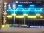
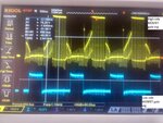
High side and Low side MOSFET Gate voltage waveform:

HO_LO Gate.jpg


Observation :

1) During high side MOSFET switching, Spike coming in Low side MOSFET Gate terminal and drain terminal.
2) If one half bridge High side MOSFET is off also, due to other bridge High MOSFET switching spike coming in remaining High side and low side MOSFET Gate terminal.
3) High side MOSFET turn ON producing more spike compared to turn off.
4) Reduced switching frequency to 30kHZ, not observed any improvement

Root cause : Noise is due to switching action
1. MOSFET switching effect due to motor coil and PCB track inductance (return path increased and cross verified, because of high inductance spike increasing)
2. MOSFET gate turn on/off time.(want to check with changing gate resistor)

Action Plan:

1) As per Easy peasy suggestion, plan to increase Ron value.

2) Plan to add snubber circuitry.

Again Verifying PCB layout with application note .

Thanks for all your suggestion, i will check and update.
 

Previous post not indicated high and low side gate signal.

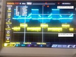
One of the bridge High and low side MOSFET gate signal :

HO_LO Gate.jpg


- - - Updated - - -

Switching noise (High side PWM Signal and Low side OFF state condition):

Spike.jpg
 

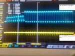
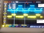
Noise in high and low side MOSFET gate terminal with 10 ohm/0.33W gate turn ON resistor : (50 percent duty cycle)
Noise with 10ohm gate resistor.jpg

Noise in high and low side MOSFET gate terminal with 82 ohm/0.125W gate turn ON resistor : (75 percent duty cycle)
Noise with 82ohm gate resistor.jpg

Observed much switching noise reduction, After increasing the gate resistor from 10 to 82ohm and reduced switching frequency to 30kHZ (82ohm selected randomly, want to analyse about gate resistor calculation). Not facing much MOSFET heating compare to last time.

Now observed less spike effect in other digital circuits connected.

Still some noise is present. I want to rectify completely. Now am working on that.

10ohm,0.1uF snubber capacitor connected across each MOSFET, not observed any improvement in switching noise reduction.

Thanks to @Easy peasy, KlausST and andre_teprom for providing useful information.
 

Hi,

I don´t think a snubber will bring much benefit. But try it.

Still I miss a lot of informations. (see post #2)
Without the PCB layout and without knowing where and how you connected the scope..I can not validate the scope pictures.
This makes it about impossible to give further assitance.

Klaus
 

You may want to slow the turn off as well, as this is where you can get inductive Vspike overshoot if you turn off too fast and there is no large decoupling cap nearby to soak up the energy - it is all very layout dependent - open wiring type layout gives a lot of headaches...

good to hear you have made some improvement...!

- - - Updated - - -

p.s. put a lot of decoupling across each fet totem pole ( if they are separated ) for a 10A motor drive @ 24VDC I suggest at least 4 x 470uF low ESR, in total, plus 1uF 100V film/foil right at the fets (from source of lower fet to drain of upper fet) - with short leads.
 
Status
Not open for further replies.

Similar threads

Part and Inventory Search

Welcome to EDABoard.com

Sponsor

Back
Top