isky
Newbie level 1
Firstly, if I am not wrong then according to my knowledge we have to maintain a specific pitch distance or multiples of it between all I/O pins while doing a physical layout designing. This is to help an auto-routing tool so that it will not miss any pins while auto-routing saving us a manual work.
Now,
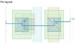
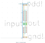
I am going to make layouts in Global Foundry's 65nm technology. Previously I have worked on IBM 130nm technology and the I/O pin pitch distance was told to us directly that it is 0.48um or multiples of it. I have attached image of inverter layout which I did in 130nm technology and also the zoomed image of its pins and the distance between them.
Now I am supposed to work on 65nm technology and I am supposed to FIND out the minimum pitch distance for this technology node.
I do not have any clue how do I do that. It's fine even if anyone doesn't tell me answer directly. Even the hint or a way to find it out would be appreciated.
Now,
I am going to make layouts in Global Foundry's 65nm technology. Previously I have worked on IBM 130nm technology and the I/O pin pitch distance was told to us directly that it is 0.48um or multiples of it. I have attached image of inverter layout which I did in 130nm technology and also the zoomed image of its pins and the distance between them.
Now I am supposed to work on 65nm technology and I am supposed to FIND out the minimum pitch distance for this technology node.
I do not have any clue how do I do that. It's fine even if anyone doesn't tell me answer directly. Even the hint or a way to find it out would be appreciated.