Continue to Site

Welcome to EDAboard.com

Welcome to our site! EDAboard.com is an international Electronics Discussion Forum focused on EDA software, circuits, schematics, books, theory, papers, asic, pld, 8051, DSP, Network, RF, Analog Design, PCB, Service Manuals... and a whole lot more! To participate you need to register. Registration is free. Click here to register now.

ALL-PMOS charge pump MOS

Status
Not open for further replies.

sa126997

Newbie level 4
Joined
May 2, 2018
Messages
7
Helped
0
Reputation
0
Reaction score
0
Trophy points
1
Activity points
49
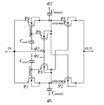
this is E. Racape and J.-M.Daga's charge pump
cp.png
4non.PNG

it use 4 Phases Non-Overlapping Clock to switch pmos P1,P5,P2,P4

if P1 and P5 are ON, P2 and P4 are OFF, else if P2 and P4 are ON, P1 and P5 are OFF.

and my question is

what are p3 and p6 work on which Active region,and p3 p6 on the function of the circuit?

- - - Updated - - -

sorry the question is p3 and p6 work on which region,and p3 p6 on the function of the circuit?
 

I'm running a simulation. From what I can see, the clock signals carry current. When P3 turns on, it connects the two lower capacitors directly in series, so that one discharges into the other. (They are joined by a common node at the Ø1 clock sources.) It looks as though it's wasteful, however it does not dissipate watts. It's a method to transfer charge.

P6 does a similar function with the upper two capacitors.

It is convenient to use Pmos because the body diodes perform a chief role at certain times in the cycle. It would not be so easy to do the same using Nmos.

The alternating clock signals provide power to the circuit, similar to applying AC.
The clock edges are unaligned, possibly because momentary shoot-through might occur if they were to coincide.
 

But vin's continuous input causes p3 and p6 to turn off, so why can they have actions?
 

But vin's continuous input causes p3 and p6 to turn off, so why can they have actions?

After a few cycles the voltage rises at the upper end of Cpump1. Soon it 'pumps up' greater than Vin, hence Vin is no longer sufficient to turn off P3. As you can see circuit operates in a manner that is not readily obvious. It's an unconventional way to use P type mosfets.
 

After a few cycles the voltage rises at the upper end of Cpump1. Soon it 'pumps up' greater than Vin, hence Vin is no longer sufficient to turn off P3. As you can see circuit operates in a manner that is not readily obvious. It's an unconventional way to use P type mosfets.

Ok
Last question is the p3 and P6 works on active region? or other region?
 

Ok
Last question is the p3 and P6 works on active region? or other region?

Several modes of operation. Vin is unchanging at the gate terminal, however the mosfets turn on or off because voltage levels change in neighboring wires.

After powerup they turn on and off in the usual simple manner, for a few cycles. The charge pump action causes voltage to rise. Vin becomes insufficient to shut off P3 & P6.

Then they conduct normally during part of each cycle, in series with the capacitors. Depending on load drain, they also may conduct in the reverse direction (upward through the body diode), sending current to the output stage (through P2 & P5 which also conduct upward through the body diode).
 

the sf coner problem

i try to make All pmos charge pump

I find that my circuit cannot reach the desired voltage in sf

BUT TT SS FF FS all reach

I checked the meaning of sf is (Slow nmos Fast pmos)

but my circuit only have pmos

little a bit strange

This is my circuit design problem?
 

A similar charge pump was posted in this thread in 2014:

https://www.edaboard.com/showthread.php?324117

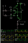
I made a simulation, which appears to work correctly. I drew one-half of the circuit to make the action easier to grasp. It boosts 10V to 17.6 at the load with 50% duty cycle.

Notice the clock signal performs much of the work since it provides most of the current which charges/discharges the capacitors. In effect it is similar to a half-bridge.

Also notice two mosfets have a fixed voltage applied to the gates, rather than being turned on and off by a pulsed clock signal. I adjusted the potentiometer so that the load voltage rose to a high level.

charge pump all Pmos 2 caps (left half) 10V to 18V 50pct duty.png

It lacks a smoothing capacitor at the load. Normally the missing half of the circuit provides the other half of the duty cycle and smoothes the output waveform.
 

    V

    Points: 2
    Helpful Answer Positive Rating
Status
Not open for further replies.

Similar threads

Part and Inventory Search

Welcome to EDABoard.com

Sponsor

Back
Top