Joeadeoye
Newbie level 6
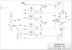
I started a Pure Sine Wave inverter project which I am to use egs002 for this purpose. I have followed the datasheet carefully. I savaged a transformer from an old ups, the transformer is 15-0-15/220v which is meant for a 24vDC 1.2kv ups. I rewind this transformer to 0-7.5/220v to use for my egs002 inverter which I believe it should give me at least 500watt on 12v system.
For a test, I used 1 fet per bridge, making a total of 4 fets, I used irf3205 and 4.7ohm resistor with 1N4148 diode at each gate, with 10k resistor from each gate-source as stated in d datasheet. I believe this bridge should give me at least 100watt power.
I connected the Ho1, ho2, Lo1, Lo2, vs1 and vs2 to their respective pins on d egs002 board, IFB is grounded and VFB is connected to an 12v additional widing of d transformer which is rectified using 4 1N4007 diodes and adjusted with a 10k variable resistor.
12v and 5v were connected to their respective pins on the egs002 board. FanCtl, TFB were left open (not connected)
I powered my circuit and connected my scope, it worked fine, I adjusted 10k pot from VFB, to get 200v ac output which worked fine. But here is the problem
I tried to connect a 20watt load for a test, immediately I connect it, egs002 will shutdown and light blinks 4 times which means undervoltage protection (as stated in datasheet). But if no load is connected, the circuit works fine and IC doesn't shutdown.
Please help me. Why is egs002 shutting down when load is connected? The load is just a 20watt light bulb