mheruian
Junior Member level 3
Proper use of PNP transistor
Hi folks,
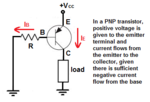
I'm actually curious about this, (still a beginner, self-studying, not a genius, doesn't have 1 year experience on electronics, doesn't have solid foundation on basics, doesn't have a mentor, always feels dizzy w/ books but always trying hard to understand this fun hobby ) I was in the process of looking for Inverted NPN darlington array transistors (at least 10) to replace my 10 PNP transistors w/o at least using inverter IC because I want it to be less spacious and few components. Then i found this picture.

I thought transistors are mostly used as simple switches (NPN = P means should input (+) to connect N and N connections; PNP = N means should input (- or gnd) to connect P and P connections). That's why I have used PNP transistors this way on the outputs of open-drain IC w/pull up resistor to drive relays or LEDs.

the above works fine together with the open-drain IC I used for a long time and nothing is wrong. Am I using PNP wrong and how it should be used? can I still use PNP on this way since it works? I hope you could please explain it to me in layman's term or as basic as possible :bang:
Hi folks,
I'm actually curious about this, (still a beginner, self-studying, not a genius, doesn't have 1 year experience on electronics, doesn't have solid foundation on basics, doesn't have a mentor, always feels dizzy w/ books but always trying hard to understand this fun hobby

I thought transistors are mostly used as simple switches (NPN = P means should input (+) to connect N and N connections; PNP = N means should input (- or gnd) to connect P and P connections). That's why I have used PNP transistors this way on the outputs of open-drain IC w/pull up resistor to drive relays or LEDs.

the above works fine together with the open-drain IC I used for a long time and nothing is wrong. Am I using PNP wrong and how it should be used? can I still use PNP on this way since it works? I hope you could please explain it to me in layman's term or as basic as possible :bang:
Last edited: