AlQadasi
Newbie
Hi all,
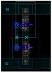
After doing some layout, I found out that the delay increase is 50%. I am getting a 6ps input-to-output delay in prelayout simulation, but getting more than 9ps delay in the postlayout simulation. The C-parasitic capacitance (between ground node and substrate) is so huge (in the 0.5fF range for some nodes) even though I am doing the layout for a simple inverter.
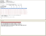
In addition, I am getting some warnings in the PEX about the layers not being mapped. Has anyone experienced this before? Is that an issue in the PDK I am using?
Thanks
After doing some layout, I found out that the delay increase is 50%. I am getting a 6ps input-to-output delay in prelayout simulation, but getting more than 9ps delay in the postlayout simulation. The C-parasitic capacitance (between ground node and substrate) is so huge (in the 0.5fF range for some nodes) even though I am doing the layout for a simple inverter.
In addition, I am getting some warnings in the PEX about the layers not being mapped. Has anyone experienced this before? Is that an issue in the PDK I am using?
Thanks
Attachments
Last edited: