Continue to Site

Welcome to EDAboard.com

Welcome to our site! EDAboard.com is an international Electronics Discussion Forum focused on EDA software, circuits, schematics, books, theory, papers, asic, pld, 8051, DSP, Network, RF, Analog Design, PCB, Service Manuals... and a whole lot more! To participate you need to register. Registration is free. Click here to register now.

Boost Converter/Frequency Response/Compensation

Status
Not open for further replies.

reann

Newbie level 4
Joined
Apr 30, 2018
Messages
6
Helped
1
Reputation
2
Reaction score
1
Trophy points
3
Activity points
68
Good day everyone!Just would like to ask some few questions.

I am currently working on a design of boost converter with the following specifications:
Input voltage =1.2V
Output voltage=2.5V
Iload=130mA (R=19.3 ohms)
switching frequency=500KHz
in a TSMC65nm technology environment.

As per calculation, I derived with the following values of inductor and capacitor with the goal to operate in CCM:

L=657uH but Lfinal=900uH to make sure it operates in CCM mode
C=19nf but Cfinal=3uF to make ripple less approximately 1%

But have difficulty as I have tested/simulated the frequency of the RLC. As shown in the attachment below:
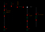
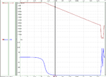
attachment2_RLC.png

attachment1-frequency_response.png

As shown above the RLC at crossover frequency (which I have chosen 1/6 of the switching frequency which is 83.3kHz). The gain needed to compensate is 58.5dB, which found to very large. To compensate. Is this value of mine realistic? If this is, can anyone suggest me what type of compensation should I used?Thank you

Btw, for now I have an operational amplifier with a gain of 70dB, phase >50 deg and UGB =10MHz.
 

Your circuit is not a boost converter. It shows the output stage of a Buck.

What you are showing is almost the control-to-output transfer function of a Voltage controlled Buck converter, not a Boost. Multiplying your transfer function by the DC input voltage would give the real control-to-output transfer function.
For a complete control of a Buck converter, you only need the PWM modulator's TF and sensor (if any) TF in addition to the already mentioned control-to-output TF. Then, you can start designing the control of the Buck.

As shown above the RLC at crossover frequency (which I have chosen 1/6 of the switching frequency which is 83.3kHz). The gain needed to compensate is 58.5dB, which found to very large. To compensate. Is this value of mine realistic?
It will be something less after you get the real control-to-output TF as explained above, but anyway still high because of large crossover.
 
Last edited:

Your circuit is not a boost converter. It shows the output stage of a Buck..

My apology for showing only the RLC circuit of my circuit. Actually, my behavioral circuit looks like this.
powerstage_boost_converter.png

As you can see from above I use an asynchronous type of boost converter, probably mistook it since my first message only shows the RLC components and not have the switches.


[/QUOTE]
For a complete control of a Buck converter, you only need the PWM modulator's TF and sensor (if any) TF in addition to the already mentioned control-to-output TF. Then, you can start designing the control of the Buck.
[/QUOTE]

Yes for my boost converter I used a PWM type of control circuit and reach the target output of 2.5V. But through the process of testing my line regulation is not good. And having sense it, I am trying to look for some solution to it, through looking the compensation part. While trying to debug, I go back to check the RLC of the boost and check the needed gain and phase to compensate it. And thats what I guess I'm having trouble since at cross over frequency I have to get a 58.5dB.

Through calculation I find that my circuit falls to a type 3B compensation.. But as tried to simulate my compensation I fail to reach the gain and phase needed to compensate the circuit.

Thats why I'm trying to find a help from everyone if you have encountered such case. Also one my collegues says that normally boosting factor should be at least 75% bigger than the input. While comparing in my specifications I have almost greater than 100% of boosting factor needed. Is that, can be a factor also?
 

While trying to debug, I go back to check the RLC of the boost and check the needed gain and phase to compensate it. And thats what I guess I'm having trouble since at cross over frequency I have to get a 58.5dB.
The RLC circuit can not predict the required transfer function for the control of a Boost converter. It can however predict the TF for a Buck (after one makes the changes explained in previous post).
In other words, using the transfer function you get from the RLC circuit for a Boost converter, you are using a mistaken frequency response in order to control the converter because it can not predict the RHP zero.

While comparing in my specifications I have almost greater than 100% of boosting factor needed. Is that, can be a factor also?
I do not know what boost factor means. Vout/Vin ?
 

The RLC circuit can not predict the required transfer function for the control of a Boost converter. It can however predict the TF for a Buck (after one makes the changes explained in previous post).

Oh, thank you for informing me, actually I have just pressumed that it would be same as buck converter. Actually this is my first hand to design a boost converter, but trying to learn it in process.
Btw , if RLC cannot predict the required transfer function for the control boost converter, is there a way that I can predict the transfer function of it?


I do not know what boost factor means. Vout/Vin ?

Yes, what I mean by boost factor is Vout/Vin.
 

Regardless what is your output spec, the boost converter is more difficult to design than a buck converter. It is not easy to predict which will be the correct combination of Volts, Amperes, step-up ratio, duty cycle, frequency, etc.

To examine action in a boost converter, consider running a slower frequency and/or a smaller Henry value in your inductor. This will produce an Ampere waveform which ramps up and down in an obvious manner.
 

Btw , if RLC cannot predict the required transfer function for the control boost converter, is there a way that I can predict the transfer function of it?
Sure.
1) Straight theory
2) Software that is able to derive transfer functions directly from the switching model of the converter e.g. PLECS, PSIM, SIMPLIS.
3) Average models..

what I mean by boost factor is Vout/Vin.
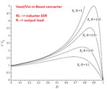
Losses in the Boost converter adds limitations to the Vout/Vin gain... however, output should be 75% bigger seems unfounded for me. Output is the necessary one, of course, making sure you can reach it. See below.

BoostFDT.png
 

To examine action in a boost converter, consider running a slower frequency and/or a smaller Henry value in your inductor. This will produce an Ampere waveform which ramps up and down in an obvious manner.

Thanks for that response. Yes, I tried to design this boost converter with a low frequency but using the formula below
formula.jpg [1]

which is the basis to at least makes the system maintain in CCM operation in which I'm trying to attain.
With that it can be seen that it would require me a bigger size of inductor (a liitle bulky). And possibly not so ideal with my application, since I'm trying to implement it in WSN apllication where in as much as possible it must be at least portable.

[1] R. Shaffer, "Fundamentals of Power Electronics with MATLAB", pg240.
 

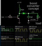
This simulation is a simple boost converter concept. 1.2V DC stepped-up to 2.5VDC. It is in continuous-conduction mode.
Inductor and switching frequency are less than values specified by your calculations above.

boost conv concept clk-driv 1V to 2_5V 130mA.png

The control circuit is not shown.
 

This simulation is a simple boost converter concept. 1.2V DC stepped-up to 2.5VDC. It is in continuous-conduction mode.
Inductor and switching frequency are less than values specified by your calculations above.

This is a pretty good value, I'm in awe.
Btw, can I ask what is the purpose of the resistor prior to the nmos/nfet switch,is it a driver? Also in your clock, can I ask what value of duty cycle you have used?
 

Btw, can I ask what is the purpose of the resistor prior to the nmos/nfet switch,is it a driver? Also in your clock, can I ask what value of duty cycle you have used?

My switching device is an ordinary BJT. The bias resistor limits current into the bias terminal. A transistor is easy to make it work at 1.2 V supply voltage.

The clock is about 62 percent duty cycle. I changed it several times, to adjust the output voltage to 2.5 V. There is a pulse generator circuit which works from two transistors, at 1.2 V supply voltage. However it is not easy to add automatic voltage regulation.
 

To get your bode plots, from which you will extract the gain and phase margin, you should.....
Multiply the Power stage transfer function by the modulator transfer function by the error amplifier transfoer function.
In fact what you do is you convert to log10 and just add them.

So eg you get gain and phase vs frequency for those three transfers.

Then , when you have added those logs you have the open loop transfer function from which you can pull out your gain and phase margin...and assess stability or the lack of it.
Remember you will have to watch the size of your source sense resistor because you could end up dropping most of the input voltage across it if not careful.
Also watch use of output diode and consider sync fet because that will be a significant percentage of your output voltage.
Are you in current mode control or voltage mode control?
Ill send you the transfer functions iif you want.
They are in Basso Book...though only you know what gains etc you have put inside the modulator in your 65nm chip.
But the power stage transfer function for eg a current mode boost shoudl be available in many textbooks......and the error amp transfer function you can calculate yourself.

- - - Updated - - -

here is one which gives power stage transfer functions
https://www.google.co.uk/url?sa=t&r...etic-control&usg=AOvVaw0f4Q7y10e_tRaiAZOUKGox

TN-203 by microsemi
Christophe Basso book is good for this though
 
  • Like
Reactions: reann

    reann

    Points: 2
    Helpful Answer Positive Rating
Thank you, i'll read it.
 
  • Like
Reactions: FvM

    FvM

    Points: 2
    Helpful Answer Positive Rating
Status
Not open for further replies.

Similar threads

Part and Inventory Search

Welcome to EDABoard.com

Sponsor

Back
Top