Continue to Site

Welcome to EDAboard.com

Welcome to our site! EDAboard.com is an international Electronics Discussion Forum focused on EDA software, circuits, schematics, books, theory, papers, asic, pld, 8051, DSP, Network, RF, Analog Design, PCB, Service Manuals... and a whole lot more! To participate you need to register. Registration is free. Click here to register now.

How can I design the OPA for LDO?

Status
Not open for further replies.

wjxcom

Full Member level 5
Joined
Sep 7, 2005
Messages
281
Helped
4
Reputation
8
Reaction score
3
Trophy points
1,298
Activity points
3,840
Hi all, I am designing a LDO which can as a power supply for SRAM. The following picture is the construction of the LDO.
There have two OPA, i.e. OPA1 and OPA2. Now the frequency of reading and writing SRAM is 60MHz, There have some questions:
1.How can I confirm the GBW of OPA1 and OPA2?
2.How can I confirm the GAIN of OPA1 and OPA2?
3.OPA1 and OPA2 are two 2-stage OPAs that have mill compensation, what's the influence of the main poles on the LDO?
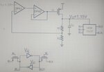
wjx1.jpg
Help me please, thanx!!
 

Why do you need 2 OPAmps? The 2nd OPAmp has no function at all, just screws the loop gain by adding an extra pole.
The 1st OPAmp probably has got 2 poles and the MOS will add an other by Cc and the feedback resistors.
This last pole have to be at higher frequency than the unity gain bandwidth of the total loop. It depends on the feedback factor of the resistors too.
 

You really want the pass transistor to be the final stage
of an op-amp-like amplifier. Trying to use "ideal" op amps
costs you stability, complexity and will give you a circuit
that is not well tailored to the gate-drive needs of the
final stage, and too slow for decent HF PSRR / load-step
tracking.
 

Hi frankrose, I don't think that the 2nd OPA has no function. In fact because of the large size of PMOS, if there have no the 2nd OPA, the pole of VG will be very small, and the stability will not be well. Now there have the 2nd OPA, the resistance of VG is 1/gm, so the pole will be large.
 

Ohh. I assume the 1/gm output resistance of the 1st OPAmp is coming from a source follower output stage.
It would be much better I think if you increased the gm somehow of the output stage in the 1st OPAmp by increasing the current consumption rather, than use an other buffer stage which adds an other pole to the system.
Or the best would be then if instead the 1st OPAmp you would use an OTA, and the large input capacitance of the PMOS would create the dominant pole of the system, and it would eliminate the 2nd OPAmp and extra poles.

Answer your questions is hard because too much things depend on others I think, there are crossings between them.
I would characterise it by this way:
1. I would assume first that the 2nd OPAmp is ideal, than the 1st OPAmp, the resistor divider and the Cc will give the stability parameters of the loop (A0, GBW, Phase- and Gain Margin).
2. When I would replace the 2nd OPAmp with a real one, the lowest pole of that buffer (with the high PMOS Cgs load) should be like 10 times higher than the 2nd lowest pole's frequency from the previous point. Thus the loop parameters (A0,GBW,PM,GM) won't change from the 1st point.
 

Do you really need an OpAmp for this? You are using Opamp plus buffer which is not beneficial as OTA + buffer= OpAmp. In fact the PMOS Cgs is low ohmic, meaning an OTA is sufficient and that should be the dominant pole for the LDO. Btw, are you sure that the regulated output is 1.15 while the reference is 1.25?!

- - - Updated - - -

In fact the PMOS Cgs is low ohmic
my mistake, high ohmic.
 

the regulated output is 1.15 while the reference is 1.25?!.
I agree, with resistor divider the output voltage will be higher than the reference voltage. I didn`t recognize that.
 

Status
Not open for further replies.

Similar threads

Part and Inventory Search

Welcome to EDABoard.com

Sponsor

Back
Top