Continue to Site

Welcome to EDAboard.com

Welcome to our site! EDAboard.com is an international Electronics Discussion Forum focused on EDA software, circuits, schematics, books, theory, papers, asic, pld, 8051, DSP, Network, RF, Analog Design, PCB, Service Manuals... and a whole lot more! To participate you need to register. Registration is free. Click here to register now.

[SOLVED] Comparator offset measurement

Status
Not open for further replies.
It's a sar adc for BLE receiver so it should be low power and its frequency is 10 MS/s, so was the comparator from this masters it was used for low power and same frequency.
 

That is fast. How much are the sizes of the input transistors, the load capacitors and the cross-coupled loads? Cannot you increase the area of them? That would help on offset, but I don't see exactly which are the main contributors for it. If you cannot find this MC result summary you can try to increase separately to increase 1 parameter, for example the width of the transistor for only 1 device with 10%, and you can check the offset in nominal, single run. Where the parameter change caused the highest offset that should be your main contributor.
 

Currently Width of 10u and Length of 300n , when I used W = 10u and length of 120n the mean of Voffset was 33mVs m but when I used W=10U & L= 300n the mean was 25 mVs, so apparently the input the transistors and MR1 & MR2 are the main contributors. WhatsApp Image 2018-03-17 at 8.21.14 PM.jpeg

I am not using any load capacitors yet ? should I ?
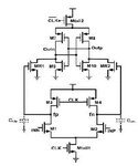
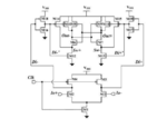
that is my schematic : Screenshot-58.png Screenshot-59.png Screenshot-60.png
 

The mean value is not relevant actually, and it really should be 0V. If the mean value is 33mV that means you haven't run enough MC or you have systematic offset (from default your circuit is asymmetric, I hope not). If you are talking about mean value it means for me that you run MC and not a single run. Please do exactly the same as what we were talking about or I will be confused and can't follow you.
I think the main contributors are the input devices (300nm is very small, of course you have n*10mV offset, increase L), and the load Cgs capacitances of NM1 and NM0. If you would use MIM or MOM capacitors instead of very non-linear MOS capacitors (Cgs of NM0 and NM1) I think that would also help on offset. Mismatch of the load caps are also relevant, and the MIM or MOM caps have smaller unit capacitance, so you could use bigger area to implement the load capacitors, thus the offset would decrease. Try to add ideal caps from analogLib as load capacitors, and check the offset. Probably it will decrease.
 
Last edited:

I am trying using another comparator : new comp.PNG where M2 & M3 dimensions are W= 1.2u 7 L =2u, and I tried a fast run of monte carlo of only 20 runs to see the range of voffset, maximum voffset was -5 mV. So I think using this circuit would be better, don't you ?
I will try to increase the width a little bit and see how much that would affect the sd in Monte Carlo of 100 runs.

Also considering your recommendation of using MIM or MOM, I am using Merged Capacitance Switching Scheme which depends mainly on capacitors , so adding a MIM or MOM capacitor will ruin the whole process and would not be fit to use under the required sampling rate.
 

Look, use it if it is better. Your target offset is extremely low, now you are still far from it. I don't think so you can reach 0.5LSB for the standard deviation with this comparator. And it would be more effective if you can use the environment and check the contributors. I am sure not only the input devices create offset.
I understand you cannot use MIM or MOM capacior, howewer I didn't say that to you to increase the load capacitance, I recommended to use linear capacitors instead of MOS Cgs loads. I would decrease the width of MOS loads and I replace those Cgs with linear capacitors. It wouldn't change capacitance on the output of the 1st stage so the sampling rate wouldn't have been touched.
 

As a practical matter, on the bench, a slow ramp is nothing
but trouble. Ground kick coupling can't be avoided and will
cause chatter anywhere near true Vio.

The industry method for piece-parts is to put the comparator
inside a measurement loop, and call the Vio the point where
the chatter duty cycle is 50%. This assumes some things
like symmetric low-overdrive prop delay, which wants some
validation (like, say, when you have an open-collector output
it's almost never true except maybe at one particular Rload).

This is a good article:
https://www.google.com/url?sa=i&rct...aw0km53zk6xC3FX8eej8hY0z&ust=1523070769853214
 
Last edited:

I think it is quite accurate and simple method to measure offset. And I don't know why you don't have Mismatch contribution in the drop-down menu. It should be under the 'Sensitivity results'. Are you sure you ticked the 'Save Mismatch Data' at the MC options?
If you want to save the signals under MC simulation you should tick the 'Save Data to Allow Family Plots'.
We don't know too much about your project to say yes you need an other comparator. We don't know the application, the speed, consumption limit, etc.

Got your point i am at the same stage while trying to getting precise measurement.
 
Status
Not open for further replies.

Part and Inventory Search

Welcome to EDABoard.com

Sponsor

Back
Top