Continue to Site

Welcome to EDAboard.com

Welcome to our site! EDAboard.com is an international Electronics Discussion Forum focused on EDA software, circuits, schematics, books, theory, papers, asic, pld, 8051, DSP, Network, RF, Analog Design, PCB, Service Manuals... and a whole lot more! To participate you need to register. Registration is free. Click here to register now.

[SOLVED] Comparator offset measurement

Status
Not open for further replies.

assemelgohari

Junior Member level 1
Joined
Feb 25, 2018
Messages
17
Helped
1
Reputation
2
Reaction score
1
Trophy points
3
Activity points
167
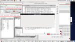
I have designed a comparator for an ADC and I want to measure its offset. All i know is to introduce a ramp voltage from 0 to Vref and on the other input a dc Vref/2 and the offset is the point at which the output switch from 0 to vdd. So I used a VPWL source and made to increase from two voltage points close to vref/2 as in the picture Screenshot-26.png . the output was as in this picture : Screenshot-27.png .
My question is : Is this a valid way to measure the comparator's offset ??

Also if I would like to know its input capacitance, what should I do ?
 

1st, yes. Better if you use long time ramp, and if your comparator has a hysteresis repeat the method with falling voltage.
Calculate the average of the upper and lower trip points, and subtitute this average from the common mode voltage, which is Vref/2 in your case (the other input's voltage). This is the offset.
The offset can be level and mismatch dependent, so you should repeat this method at different common mode levels, not just Vref/2, and run Monte Carlo mismatch simulation.

2nd, to get Cin connect the inputs together, and apply a DC voltage level to them (for example Vref/2). Probably in this case all input devices are in saturation and the Cgs capacitances are maximal. Set the AC magnitude of the vdc source to 1V, and run AC simulation. Measure the current of the input pins of the comparator, and you can calculate Cin_P an Cin_N:
Cin_P=mag(IF("/vinp"))/(2*3.14*xval(IF("/vinp")))
Cin_N=mag(IF("/vinn"))/(2*3.14*xval(IF("/vinn")))
vinn and vinp are the input pins of the comparator. Try to set different DC levels to check the capacitance at other common mode input levels.
 
Last edited:
1st, I have tried a longer ramp for a larger input range, but then i started narrowing the range to get an accurate result. I don't how to identify if my comparator has a hysteresis or not ? but you mean to repeat this test with a falling down ramp ?
Considering your second paragraph:
you mean to get at which part the output value switch in the rising ramp like this :

**broken link removed** ( this is the same previous image but zoomed in )
and then repeat this test with a falling ramp and then get the average between them ?and this average is the offset ? Also Is it possible to show you my monte carlo results to confirm if I have done it a valid test ?

2nd, My input devices are not in saturation at Vref/2 so do I have to find a DC value which ensures that they are in saturation ? or change in my circuit to make them in saturation at Vref/2 ( and other common mode input levels as you've suggested) ?

3rd, Is there a simple test to measure the kickback noise ?
 

Youar attachment is not valid.

Anyway yes, do a ramp-up and a ramp-down in transient analysis. Slower ramps give more accurate results.

How to identify the hysteresis? Do a ramp-up and after it a ramp-down, and if the trip points are not the same your comparator has got a hysteresis.

You can calculate the offset like this: https://www.maximintegrated.com/en/images/appnotes/886/886Fig01.gif
I know 2 definitions of offset actually, 1st is the commonly used maybe, by the attached picture, which is yes, the average of the trip points, and the 2nd definition is the shift of the hysteresis window. I described this in my last post. It also contains the averages of the trip points, but the common mode level is subtracted from the average to get the exact shift of the hysteresis window.

I don't know your circuit, if it works well as a comparator don't change anything just because your inputs are not in saturation. Choose a DC level from the valid input range where the input capacitance is the highest. Smaller capacitances are not relevant to ensure the specifications.

There is no kickback noise I think, just kickback. Kickback can cause problem if your input sources have high output resistance, and/or the inputs of the comparator are coupled capacitively. So to test add source resistances and measure the comparator delay change.
 
I am trying to first get the upper trip to get the offset using monte carlo , so i added to the output Voffset which expression is :value(wave_17() cross(wave_16() 0.65 1 "either" nil nil ) ) ... where wave_16() is the voutput differential so I am getting when would it cross threshold voltage of 0.65,, and wave_17() is the vinput differential, which gets me the upper trip .. but the monte carlo test is not running. I have added the monte carlo file as in this image : Screenshot-31.png

and I keep having this error ? as in this image Screenshot-29.png stating no statistical data generated for the test.
 

Attachments

  • Screenshot-30.png
    Screenshot-30.png
    133.6 KB · Views: 598

What is in the error log? At the virtuoso CIW winndow, or somewhere else you can read more maybe.
Try to import the model library at the Data Window/Corners, maybe that is the problem you try to use too much model definition at Nominal corner.
 

I fixed it, now I want to know how to know what are my limitations in the offset matter ? I mean what is the maximum offset I have to design the comparator below if I am designing this comparator for an 11-bit SAR ADC ( 10 MS/S ) ? and vref =1 V

- - - Updated - - -

I want to know for both dynamic and static offset error ?
 

Offset should be small as possible, but there are trade-offs between the current consumption, area and speed. Thumb rule is that offset should be maximum 0.5 LSB, 250uV if 1V is the full scale voltage, for the standard deviation.
 
Last edited:
I am doing this test I have previously mentioned of input ramp from 490mv to 510mv in one input and the other with dc value at 500mv and check when the voutput differential will switch and this is Voffset. when i run it in nominal situations Voffset is in microvolts, However when i run it in monte carlo Voffset is most of the times Voffset is = -10mV , and the voutput differential switch at the beginning of the test ? as in this image Screenshot-51.png

and the monte carlo output is not logical or I can't understand Screenshot-50.png Screenshot-49.png

while the nominal run output is : Screenshot-47.png Screenshot-48.png

Voffset expression is : value((v("/in+" ?result "tran") - v("/in-" ?result "tran")) cross((v("/out-" ?result "tran") - v("/out+" ?result "tran")) 0.65 1 "either" nil nil))

and now I am trying to increase the input ramp to be 450mv to 550mv.
 

I think you are doing it well, the expression can be good and I don't understand what is your problem. It is normal the offset is in uV range over process/voltage/temperature variations and reaches X mV in mismatch simulation.
 

Nominal run: The model file used for the nominal run (tt) usually doesn't provide an offset parameter (wouldn't make much sense, as the (mainly vth) differences are distributed around 0±offset). So the comparator switches after the first active (negative) edge, and the calculator expression just provides a delay+skew time difference value between Vindiff(active edge) and Voutdiff(rising) to cross half (?) the supply voltage.

Monte Carlo run: The N=40 vth-offset runs show a good frequency distribution around zero; the N=35 voffs frequency distribution the most often ocurring values between -8..-10mV (and a max. voffs value < |8.4|mV), however with a relatively high sigma value (half the max. value!) - because of these few runs, of course.
 
erikl : considering the failure in the test in monte carlo was because of a glitch that happens at the beginning of the simulation resulting in voutput differential to be 1.2V in the beginning and while falling my Voffset expression took it as its value,
Screenshot-53.png
so I changed Voffset expression to be : ( when voutput differential rise in only a rising edge only to a 0.65, capture the value of vinput differential as Voffset) Voffs = value((v("/in+" ?result "tran") - v("/in-" ?result "tran")) cross((v("/out-" ?result "tran") - v("/out+" ?result "tran")) 0.65 1 "rising" nil nil))
and it works correctly now, but the voffset is in mVs, so my questions for you are : what is the upper limit to my comparator if it is used for 11-bit SAR ADC with vref=1V ? and how to calculate it ? how to calculate the maximum this ADC can tolerate ?

How did you deduce this info or data from the photos I previously posted ? how did you knew that when N=35 voffset was in that range ?


frankrose :
I figured out what was the problem and I explained it previously in this reply, my questions to you are : how can be the offset to be in mVs and my LSB is around 400 uVs ? won't this offset ruin the 11-bit SAR ADC process ? and also what is my upper limit ? how to calculate the maximum I can tolerate ?
 

erikl : the two images I posted for the Monte Carlo were from the same simulation. one was for Voffset and one for the change in vth of the transistors used ( not sure about that )
 

what is the upper limit to my comparator if it is used for 11-bit SAR ADC with vref=1V ?
As frankrose told you in post #8: ≦ 250µV (for ADC_output-range = 1V. Exactly ≦ 244µV ).

how to calculate it ? how to calculate the maximum this ADC can tolerate ?
≦ ½LSB = 2-(N+1)*ADC_output-range . N is your ADC's resolution.

How did you deduce this info or data from the photos I previously posted ? how did you knew that when N=35 voffset was in that range ?
It's in the image's insert: mu & sd

erikl : the two images I posted for the Monte Carlo were from the same simulation. one was for Voffset and one for the change in vth of the transistors used ( not sure about that )
You're right!
 
WhatsApp Image 2018-03-17 at 8.21.14 PM.jpeg I am using this comparator and I think that M1, M2, MR1 & MR2 are the main contributors in the offset, so as offset is Av/sqrt(W*L) I have used large W ( 12um ) for the four transistors but I am still getting a very large sd for the Voffset as in this picture around 32 mVs. I am far away from my upper limit , so what I should or can do to enhance this voffset to be in uVs ? increase the L too ? use an offset cancellation technique ? use another circuit for the comparator ? Screenshot-54.png . Also I want to know what is the difference between static and dynamic offset ? and which one I am measuring ? and which one is ruled by the upper limit You have just mentioned ?
 
Your new offset statistic shows unbelievingly high values - and doesn't fit with your former N=35 representation. I think your offset measurements should be below |10mV|, mostly in the order of only a few milliVolts. Anyway, also if you succeed to achieve a mV offset range, for such high resolution (and your ADC topology) I think you would need offset cancellation or even individual trimming.

There are other ADC architectures which don't need ½LSB comparator resolution - check e.g. the RSD topology.

The difference between static and dynamic offset is just the speed of changing the input voltage difference: if you use a slowly changing - compared to the reaction time - linear ramp, you measure the static offset. By using a fast-edge stairCase you get dynamic offset.
 
My formerm N =35 graph as I have told you before was not monte Carlo for Voffset, It was for the change of Vth of transistors. you can check the label or title of the graph, you would find one label Voffs and the other is of vth of the transistor.
I don't know why I have such high sigma value, When I tested this comparator through an overdrive test as this Screenshot-25.png comparator was able to detect even nano volts. Also when I run the offset test I have mentioned that I am using in the nominal case or not in monte Carlo the offset was in uVs as in post#9 . However in Monte Carlo the number varies greatly and not logically, that's why I am suspicious and feel that there is something wrong in the test or the monte Carlo setup to give such output as in this image : Screenshot-56.png .

If there is, what would I double check to make sure that my test is valid. or Is there another way to measure my offset in an accurate and simple way ?

Also, I would like to ask what topology or comparator's circuit would you recommend for high resolution and low power ?
 

To find the main contributors of the offset you can do this:
1. Right to the "Monte Carlo Sampling" there is green symbol for the MC settings. Set the sample number to 1000, choose Latin Hypercube sampling and tick 'Save mismatch data'. Don't choose process variation, only mismatch.
2. Run the 1000 simulation.
3. At the Data tab on the left there is an other tab, the 'History'. Click on it and click with right button to your last MC run. There should be a 'Mismatch contribution' in the drop-down menu.
4. Click with right button on the 'voffs' column and sort by that value
With these you can find out which are your problematic devices. Also check your transient curves manually where the offset is huge and it can make you confident that your measurment method is good.
 

Capture.PNG I could not find mismatch contribution in the drop down menu as you can see in the previous Image, but in the next Image I have opened mismatch results & sensitivity results. I could not understand what do you want from me to deduce or come up from these results as I don't understand what do these results show me? Screenshot-57.png
4- I am not able to reach the transient curves, when I get the Details from Monte Carlo and I putting Voutdifferential and Vinput differential from the outputs, I am not able to plot the wave, when I press right click and choose plot all, I find ( plot all ) unselectable. I am only able to plot the last run from the results Screenshot-56.png .

should I try another comparator ? I have found a Masters that used one for a 10 bit SAR ADC, but it did not include offset simulations. Should I try this circuit and see if the problem was due to error in my test ? or the problem from the circuit ?

Do you recommend any other test for accurate offset measurement ?
 

I think it is quite accurate and simple method to measure offset. And I don't know why you don't have Mismatch contribution in the drop-down menu. It should be under the 'Sensitivity results'. Are you sure you ticked the 'Save Mismatch Data' at the MC options?
If you want to save the signals under MC simulation you should tick the 'Save Data to Allow Family Plots'.
We don't know too much about your project to say yes you need an other comparator. We don't know the application, the speed, consumption limit, etc.
 

Status
Not open for further replies.

Part and Inventory Search

Welcome to EDABoard.com

Sponsor

Back
Top