Continue to Site

Welcome to EDAboard.com

Welcome to our site! EDAboard.com is an international Electronics Discussion Forum focused on EDA software, circuits, schematics, books, theory, papers, asic, pld, 8051, DSP, Network, RF, Analog Design, PCB, Service Manuals... and a whole lot more! To participate you need to register. Registration is free. Click here to register now.

Balanced OTA-C cascode IC design

Status
Not open for further replies.

sherif96

Member level 4
Joined
Feb 22, 2018
Messages
77
Helped
0
Reputation
0
Reaction score
0
Trophy points
6
Activity points
732
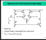
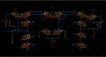
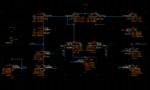
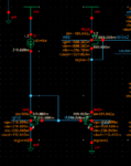
I am designing a balanced ota with cascode output stage attached is the circuit in a textbook and my ota schemaitc, however I am still new to IC designing I did not get the hang of all the basics yet, I am trying to bias all the transistors in the circuit and due to the assymetric second stage transistors I decided to adjust my circuit to be fully differential and add an extra common mode feedback circuit, to make the circuit fully differential i removed the current mirror in the real circuit at the bottom right, to have two identical branches - correct me if i am wrong- however the circuit is not biased correctly yet and some of the vdsat numbers are very high, any ideas?
vdd=1.2v
vn5=500mv
vp5=500mv
vn6=250mv
vp6=250mv
 

Attachments

  • IMG_20180312_093911.png
    IMG_20180312_093911.png
    100.7 KB · Views: 140
  • OTA.png
    OTA.png
    36.4 KB · Views: 202

Don't design a full-differential OTA just because the output stage is asymmetric. Point of fully differential circuits is they have good common-mode and supply noise rejection. With good supply and bias it is just much harder to design a fully differential OTA then an asymmetric output amplifier.
And there is no common-mode feedback circuitry above. Those pull-up PMOS devices just can't leave the output to go any lower voltage levels.

i am applying the differential circuit as the output swing with the cascode devices is very low, differential circuit would boost my output swing a bit, why isnt the circuit above common mode feedback? shouldnt it be ideally a vcvs with my reference voltage as input which in my case is vdd/2 and my output voltage and feedbacking the output of the vcvs to the branch once again ?
 

Differential output doesn't mean higher swing. Asymmetric output should have got same voltage range.
I have already written why not common-mode feedback that what you shown. You just added pull-up devices. When you control it differentially your pull-ups won't let the output to go down. This is not a common-mode sense circuitry.
 
Hi,
I hope you noticed that one of the diode connected PMOS has the bulk to gnd!. This is bad.
I don't think your CMFB circuit si working. You can use two resistors as cmfb, as shown in the images below, to verify your bias. Pls note that the values of the resistors are prety high, and this configuration isn't used to much in practice.

pQwJXaZ.png

YUHftGo.png
 
Well i managed to implement the CMFB circuit as attached and my vout+ and vout- are around vdd/2 now ideally using a vcvs and two resistors as shown in the second attachment, however I am having some trouble designing the opamp which would replace the vcvs, i have designed the ideal vcvs using a gain of 100, however the output gain from the opamp is messed up,also in regards to the ac analysis how would the gain of the opamp appear in ac analysis if the voltage input vavg is almost a dc of 600 and the other input vref is always dc, how can the opamp gain be designed with the previous conditions?
 

Attachments

  • CMBF.PNG
    CMBF.PNG
    39 KB · Views: 127
  • Ideal opamp.PNG
    Ideal opamp.PNG
    23.8 KB · Views: 126
  • Gain.PNG
    Gain.PNG
    53.2 KB · Views: 120

i have designed the ideal vcvs using a gain of 100
The CMFB amp doesn't need such high gain.

however the output gain from the opamp is messed up
... 'cause you load its output impedance of perhaps 5..10MΩ with a much lower impedance for the vavg generation.
 

The CMFB amp doesn't need such high gain.


... 'cause you load its output impedance of perhaps 5..10MΩ with a much lower impedance for the vavg generation.

- when i use a lower gain the accuracy of the voltages vout+and vout- decrease , I want them to be vdd/2 however when i use gain of 50 for example their voltages go from 602mV to around 700, in the second comment you mean I am using a 1M ohms when i should be using a much higher resistance ?
 

Won't be enough to increase the resistance if you want to connect the common mode feedback circuitry to the differential circuit.
I think you want to connect the asymmetric OTA's output to the 'vcmfb' nodes of the differential OTA. But your asymmetric OTA's NMOS tail current source will be in triode region. You should implement an other asymmetric OTA with PMOS tail current source.

I think I got lost in the middle, to conclude you mean I should use a PMOS tail current source and implement changes to my circuit to work with it rather than my NMOS tail current source?
 

Won't be enough to increase the resistance if you want to connect the common mode feedback circuitry to the differential circuit.
I think it would help. Let's give it a trial.
On the other side, much higher resistor values (e.g. 10MΩ) use a lot of silicon area.

your asymmetric OTA's NMOS tail current source will be in triode region.
No, NM8 is in saturation region (region=2): vds > vdsat

You should implement an other asymmetric OTA with PMOS tail current source.
Against what should this help? Simply the other way round?

BTW: Why do you speak of asymmetric OTA? Where do you see asymmetry?
 

He is using a non-differential OTA (=asymmetric output) to create common-mode feedback for his differential OTA.
The common mode feedback input of his differential OTA are the NMOS current sources at the bottom (NM1 and NM4).
If he wants to control those NMOS gates I think a PMOS input, single-ended (=asymmetric output) OTA should be implemented.
NM12 and NM11 won't be in saturation if he connects the drain of NM11 to the CMFB input of the differential OTA.
You misunderstood me, NM8 is not affected, I didn't talk about that amplifier. The single ended OTA (=asymmetric output) will have problems.
 

He is using a non-differential OTA (=asymmetric output) to create common-mode feedback for his differential OTA.
Oh, you thought of the CMFB-amp. Sure, clear.

The common mode feedback input of his differential OTA are the NMOS current sources at the bottom (NM1 and NM4).
Right.

NM12 and NM11 won't be in saturation if he connects the drain of NM11 to the CMFB input of the differential OTA.
Understand now: Because of the ≈900mV CMFB output voltage mismatch to the ≈300mV required CMFB input voltage.

If he wants to control those NMOS gates I think a PMOS input, single-ended (=asymmetric output) OTA should be implemented.
Yes, you're right. Would probably fit better.

You misunderstood me, NM8 is not affected, I didn't talk about that amplifier. The single ended OTA (=asymmetric output) will have problems.
My misunderstanding, sorry. Always thought you were speaking of the main OTA - because I'm used to call the other one the CMFB-amp.
 

If you do not mind, I just got lost between the different nominations, I understand that my problem is as frankrose mentioned that my CMFB amplifier or my assymetric ota's nmos current source will not be in saturation, but I did not quite understand the solution through the different nominations in the replies, is it that I should replace my NMOS current source in the CMFB amplifier with a PMOS one?
 

No problem man. But the 'Because of the ≈900mV CMFB output voltage mismatch' sentence sounds like a science fiction. Simply the output voltage swing is limited.

sherif96:
An NMOS input non-differential OTA has a limited range for output swing: Vo.max=VDD-Vdsat.load, Vo.min=Vcm-Vgs.in+Vdsat.in
The Vo.min in your case is 600mV-293mV+72mV=379mV. So the output can't go down to 292.558mV, this is your CMFB input voltage in your differential OTA.

You should use a PMOS input non-differential OTA, because the Vo.min=VSS+Vdsat.load, which should be less than 293mV.

You should design an OTA like this: http://www.ijoart.org/papers/A-LOW-...SIGN-USING-018M-CMOS-TECHNOLOGY/Image_004.png
 

the 'Because of the ≈900mV CMFB output voltage mismatch' sentence sounds like a science fiction.

A misunderstanding, again: The actual CMFB quiescent output voltage was meant: sherif-CMFB-amp.png
 

well I implemented the PMOS tail current source ota and the gain plot is fixed and the biasing is ok, however there is something I do not quite understand, the ideal cmfb- the vcvs in the first attachment- has two inputs vavg which is the sensing output from the differential outputs and a dc voltage which is vref vdd/2, how should I connect them to the non differential cmfb amplifier since there will not be a +ve input differential or even a negative one? I am asking because the non ideal circuit behaves not as the ideal circuit does, the ideal circuit outputs around 200mV and upon increasing gain both differential outputs gets closer to vdd/2, however the non ideal circuit if i increase the gain the cmfb goes even further and if I try to connect it the differential ota it does not perform as intended to do obviously, any idea what went wrong ?
 

Attachments

  • PMOS cmfb.PNG
    PMOS cmfb.PNG
    26.1 KB · Views: 94
  • Current Mirror.PNG
    Current Mirror.PNG
    12.5 KB · Views: 111
  • Gain.PNG
    Gain.PNG
    60 KB · Views: 93

Did you connect the common mode feedback output of the CMFB amplifier to the differential amplifier's common mode feedback inputs?
 

But why would I connect the cmfb amplifier of the non ideal circuit to a different input than the one i chose and designed for the ideal circuit? What is the difference between connecting at the bottom transistors as I did the photos attached in a previous post and what you are asking me to do? Shouldnt both work fine just differs in the transistors parameters for correct biasing?
 

Explain us why you don't want to connect the 2 circuits as attached below? The yellow circled wires should be connected together I think.
5ZZyt90m.png
luI13G6m.png
 
Last edited:

Status
Not open for further replies.

Part and Inventory Search

Welcome to EDABoard.com

Sponsor

Back
Top