Continue to Site

Welcome to EDAboard.com

Welcome to our site! EDAboard.com is an international Electronics Discussion Forum focused on EDA software, circuits, schematics, books, theory, papers, asic, pld, 8051, DSP, Network, RF, Analog Design, PCB, Service Manuals... and a whole lot more! To participate you need to register. Registration is free. Click here to register now.

MCU does not boot on power up, only starts when reset button is pressed

Status
Not open for further replies.
Okay, so I reiterate what was said before.
Increase the RC time constant of the reset so that nRST goes up just after Vcc got steady.
 

Hi,

Here are the transient responses where yellow is the input voltage and blue is the reset voltage
This makes no sense to me.
Usually the RESET circuit is supplied by the same supply voltage than the microcontroller.
But in your case the RESET output voltage is higher than the supply voltage.

Are you sure you didn´t mix the colors? --> blue= supply, yellow = RESET

Klaus
 

Hi,


This makes no sense to me.
Usually the RESET circuit is supplied by the same supply voltage than the microcontroller.
But in your case the RESET output voltage is higher than the supply voltage.

Are you sure you didn´t mix the colors? --> blue= supply, yellow = RESET

Klaus

Yes, that's right, it is vice versa. I wrote it wrong.
 

In a forum post, I read that noise in oscillator may cause the oscillator to lock and prevent the MCU booting unless reset is applied.

I checked my oscillator behavior and sow that I have a noisy oscillator compared to my previous design. So, do you have any suggestions based on this?

Thanks,
Ogulcan
 

Hi,

How did you measure the "noisy" oscillator? Show the measurement results.

Best is to keep on the datasheet recommendations.
* Read the microcontroller datssheet oscillator section
* read the XTAL datasheet

Additionally you need to use a good PCB layout with solid GND plane, power supply capacitors next to each power supply pin, short wiring to the XTAL, low impedance connection of XTAL_capacitors to GND.
This safes from noisy / unreliable oscillator clock.

Klaus

You can see it by oscilloscope, but when you take the screenshot, there is not much difference, but there is a significant difference when you see it in real. I need to take a video I guess.

I tried to do my best for the oscillator in general. But there are too much signal lines around. I put as much via around oscillator as possible but I guess it did not help.
 

Hi,
You can see it by oscilloscope, but when you take the screenshot, there is not much difference, but there is a significant difference when you see it in real. I need to take a video I guess.
you have a ROHDE & SCHWARZ scope...it should be no problem to show us what you mean.

I tried to do my best for the oscillator in general. But there are too much signal lines around. I put as much via around oscillator as possible but I guess it did not help.
This is no useful information. Neither for us nor does it help you with your problem.
Why don´t you show us your PCB layout? Too secret?

Klaus
 

Hi,

you have a ROHDE & SCHWARZ scope...it should be no problem to show us what you mean.


This is no useful information. Neither for us nor does it help you with your problem.
Why don´t you show us your PCB layout? Too secret?

Klaus


It's not problem when I share partially.

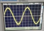
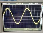
I shot videos and converted them to GIF, here are the oscillator screens:

Old design:
old-design-osc-photo.jpgold-design-osc-gif.gif

New design:
new-design-osc-photo.jpgnew-design-osc-gif.jpg

I''ll send PCB's in an hour.
 

Hi,

your scope pictures:

I assume this is not a true oscillator problem.
* check if this isn´t just a measurement error (introduced by the scope or the scope cabling, for example)
* check power supply stability
* maybe induced from an SMPS... in burst mode?
* your cellular phone or any other HF source like WLAN, Bluetooth....

Klaus

I've checked this several times and also different days while the PCB's are in the same environment.

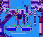
Here is the PCB near crystal:
TOP:
osc-top.JPG

BOT:
osc-bot.JPG

Thanks,
Ogulcan
 

Hi,

it seems like a two sided PCB. Difficult to route. Can´t you move to a 4 -layer PCB?

I personally don´t like a "copper fill" used as GND plane. Because it is far a way from being a solid - low impedance - GND plane.

You see the GND is splitted in many pieces on both sides. For sure you tried to connect them with a lot of vias.

One example is in the picture.
power.jpg
You see the pins: GND and VCC next to the oscillator pins. Most probably these are the supply pins for the internal oscillator_inverter.
I tried to find the shortest (HF) connection between this VCC and the corresponding GND pin. It changes layer (via) four times and encloses a relatively large area. The size of the area is a measure for EMC (and EMI) . The connection loop is of inductive character... with a series connected C ... creating an LC resonant.

I don´t think that this is causes the problem. ... but there´s a chance for it.

***
For your next 2-sided PCB:
Do the placement according schematic. To get shortest connections between parts.
Try to put the GND plane to the bottom (red) side. Try to route as much signals as possible on the top (blue) side. Only short pieces of signal on the bottom side. Try to keep GND plane as solid as possible.
In your PCB .. rotating the pin header by 180° (if possible) may avoid a lot of signal in the bottom layer.

But I know: often things are not as easy as they seem..

Klaus
 
Hi,

it seems like a two sided PCB. Difficult to route. Can´t you move to a 4 -layer PCB?

I personally don´t like a "copper fill" used as GND plane. Because it is far a way from being a solid - low impedance - GND plane.

You see the GND is splitted in many pieces on both sides. For sure you tried to connect them with a lot of vias.

One example is in the picture.
View attachment 144753
You see the pins: GND and VCC next to the oscillator pins. Most probably these are the supply pins for the internal oscillator_inverter.
I tried to find the shortest (HF) connection between this VCC and the corresponding GND pin. It changes layer (via) four times and encloses a relatively large area. The size of the area is a measure for EMC (and EMI) . The connection loop is of inductive character... with a series connected C ... creating an LC resonant.

I don´t think that this is causes the problem. ... but there´s a chance for it.

***
For your next 2-sided PCB:
Do the placement according schematic. To get shortest connections between parts.
Try to put the GND plane to the bottom (red) side. Try to route as much signals as possible on the top (blue) side. Only short pieces of signal on the bottom side. Try to keep GND plane as solid as possible.
In your PCB .. rotating the pin header by 180° (if possible) may avoid a lot of signal in the bottom layer.

But I know: often things are not as easy as they seem..

Klaus

I'll try to follow your recommendations if I need to redraw my PCB, but as far as I understand, this problem is not really caused by the crystal (although it can be improved), maybe it affects, but it's not the main problem.

What do you mean by this?
In your PCB .. rotating the pin header by 180° (if possible) may avoid a lot of signal in the bottom layer.
 

Hi,

I'll try to follow your recommendations if I need to redraw my PCB, but as far as I understand, this problem is not really caused by the crystal (although it can be improved), maybe it affects, but it's not the main problem.
correct.

What do you mean by this?
power2.JPG

Klaus


So you mean the signal lines are better not connected angled, instead they should be connected 180 degrees to prevent distortion, EMI etc.

I've bypassed my power stage and connected 3.3V directly to my 3.3V node, and guess what? The crystal distortion problem is solved in this scenario. So this means my power stage is not filtering the good enough, I'll try to improve this.

However, the power up booting problem is not solved in this trial, this is happening due to another defect apparently.

Thanks,
Ogulcan
 

Hi,

So you mean the signal lines are better not connected angled, instead they should be connected 180 degrees to prevent distortion, EMI etc.
????
This has nothing to do with distortion or EMI.

Just rotate the pin header (not the angles). Then the right most signal becomes the left most signal and vice versa...
...then you can route almost all signals on the top side. Thus the bottom side GND plane becomes more solid..

Klaus
 

Hi,


????
This has nothing to do with distortion or EMI.

Just rotate the pin header (not the angles). Then the right most signal becomes the left most signal and vice versa...
...then you can route almost all signals on the top side. Thus the bottom side GND plane becomes more solid..

Klaus

I cannot do that, because that's actually an LCD and rotating it rotates the LCD.

Ogulcan
 

Hi,

I now have C7 as 10uF and R15 as 100k ohms.

Remember the circuit:
rst.JPG

Here is the response to power up:
power-up-rsp.jpg


Do you think I should increase the time constant even more?

Thanks,
Ogulcan
 

Hi,

I don´t think that increasing the time constant solves your problem.
The calculated tau is 1s, but in the scope picture it is only about 300ms. Is there another pullup?

***
My recommendtion:
* write a debugging code that just toggles a pin.
* program your controller with it.
* power down
* power up
* see if pin toggles
---> If not toggle: measure all supply voltages and reset pin voltage (all with DVM and all with scope) and write the values down. Measure clock output signal with a scope and take a photo.
Then press the reset button for a shrt time
Then again measure all supply voltages and reset pin voltage. Measure clock output signal with a scope and take a photo.
Compare all the values ... there should be a a difference.

--> if it toggles: Then modify your original code with some debuging features (set, clear toggle pins) to find out where the software hangs.

****
In your first post you write: "I does not boot automatically, yet when I press the reset button, it boots."
How do you detect this? By seeing a blank display?
Could it be a timing problem on initializing periferals?
Or something else....

Klaus
 
The calculated tau is 1s, but in the scope picture it is only about 300ms. Is there another pullup?
No, there is no other pullup, I measured it with multimeter, but maybe there is some other connection to Vcc through RST pin inside the MCU, who knows :)

In your first post you write: "I does not boot automatically, yet when I press the reset button, it boots."
How do you detect this? By seeing a blank display?
Could it be a timing problem on initializing periferals?
Or something else....
Klaus
I have a starting tone, I have LCD, RS232 everything, basically I can understand that it boots.

I've actually done many software developments since this board had arrived, but I didn't focus on this apparent problem, I postponed it. So,I know that peripherals are okay, but I'm not sure if a peripheral makes the MCU hang during power up.
 

Hi,

but maybe there is some other connection to Vcc through RST pin inside the MCU, who knows :)
... this was my question...
--> datasheet knows.

I have a starting tone, I have LCD, RS232 everything, basically I can understand that it boots.
If I understand correct, then the problem is that it doesn´t boot.
So let´s focus on the situation when it does not boot.
--> how do you detect this situation?

Are you 100% sure that the MCU doesn´t perform a single instruction?
If you are less than 100% sure then please follow my recommendation of post #38.

Klaus
 

Status
Not open for further replies.

Similar threads

Part and Inventory Search

Welcome to EDABoard.com

Sponsor

Back
Top