Continue to Site

Welcome to EDAboard.com

Welcome to our site! EDAboard.com is an international Electronics Discussion Forum focused on EDA software, circuits, schematics, books, theory, papers, asic, pld, 8051, DSP, Network, RF, Analog Design, PCB, Service Manuals... and a whole lot more! To participate you need to register. Registration is free. Click here to register now.

ADS Layout , no EM models, Ground problem

Status
Not open for further replies.

xzsawq21

Junior Member level 1
Joined
Jul 23, 2011
Messages
16
Helped
0
Reputation
0
Reaction score
0
Trophy points
1,281
Activity points
1,407
Hello
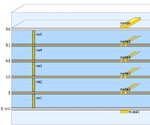
I have a passive filter with a 6-layers PCB.
this is the substrate:
3.JPG
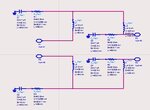
I have drawn the schematic in ADS using Lumped-with Artwork and simulated it.
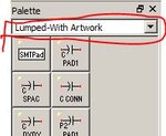
1.JPG2.JPG

then using Generate/update Layout, I transferred it to a layout as shown below:
(plus I have used rectangular with 20 mils clearance)
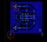
4.JPG

but I have some problems with EM simulation:

when I double click on the vias:
6.JPG
is it right for a 6-layers PCB?


no EM model:
4.JPG

would you please give me an straight answer?

Best Regards
 

The ports of RLC components are "Layout Purpose Only" not for EM Simulation.Therefore ADS cannot find any model for them.
Instead, you should place a "Port" for each component's Pin and do your EM simulation then attribute a component model ( linear or SPICE based) for each component.
So, you have to do Co-Simulation with these components in Schematic Simulation Environment.GND Port is particularly used for some problems otherwise GND is common for all components.Don't place GND Port in EM Simulation mode.

Dear
Thanks
you mean I should use "lumped-components" in schematic instead of "Lumped-with Artworks"?
How should I attribute models?
I watched the below video before
https://www.youtube.com/watch?v=v0OMSx1vLnc
I did like him but there is no SMD models for Resistors, Capacitors, Inductors in ADS design Libraries.
 

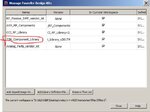
I have downloaded some ADS libraries and unzipped it and checked the definition files.
then I drew a schematic as shown below:
test.JPG

but when I want to simulate it I see this error message:
test.JPG

what should I do?

I couldn't find well documented tutorials for ADS. most of Keysight's tutorials are advertisement.

Thanks
 

For the designkit components, you often need an INCLUDE element that tells ADS to include the library definitions. Check the component palette of your library.
 

For the designkit components, you often need an INCLUDE element that tells ADS to include the library definitions. Check the component palette of your library.

Thanks
Do you see any problem?
1.JPG2.JPG
I have chosen all the components from the Palette.
 

As I wrote above: you also need to place the "TDK netlist include" on your schematic. That is the first component in your palette (top left).
 

As I wrote above: you also need to place the "TDK netlist include" on your schematic. That is the first component in your palette (top left).

OK :) Thanks
I have set a 6-layers substrate as shown below:
1.JPG

as you see I should mount the components on the top side (metal6) but when I want to transfer it to layout:
3.JPG

2.JPG

I want to route some tracks on the top side, but the components don't have some pads on the top side! I tried to change the pad layer but I couldn't do it.
would you please help me.
 
Last edited:

I have never used that library, but have you tried to do what the message says?

Looking at that default color, it looks like you have some SMD pads on layer cond? And the TDK pads on other layers?
 

I have never used that library, but have you tried to do what the message says?

Looking at that default color, it looks like you have some SMD pads on layer cond? And the TDK pads on other layers?

Dear
Yes, I think I should set something in schematic to set these components at top layer
I have opened an example from default path in ADS's folder:
C:\Program Files\Keysight\ADS2016_01\examples\Training\Layout
actually they have used symbols instead of prepared models (Design Kits) as shown below, so they could set the layer as you see:
1.JPG

But I have used prepared models (Design Kits) by vendors, but I don't know how I should define the layers.
the error is:
2.JPG

in below topic I found something:
https://www.edaboard.com/showthread.php?t=292488
this is one of pics in his topic:
3.JPG

- - - Updated - - -

I'm sorry I couldn't edit my message, eventually I could find the SMT_PAD,
1.JPG
but I have a new problem!

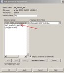
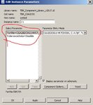
as you see I could set the SMT_Pad for the resistors bcoz in resistor's property I can access to this parameter as shown below:
2.JPG

but for the capacitor there is no such parameter in its property:
3.JPG

how should I add "SMT_Pad" parameter in capacitor's property?
Thanks
 

It seems that the TDK library does not use SMT_PAD for layer settings, that is only for the ADS built-in elements.
I don't know how TDK components set the layers. Maybe in the "TDK netlist include" element? Is there documentation for that library?
 

Status
Not open for further replies.

Part and Inventory Search

Welcome to EDABoard.com

Sponsor

Back
Top