Continue to Site

Welcome to EDAboard.com

Welcome to our site! EDAboard.com is an international Electronics Discussion Forum focused on EDA software, circuits, schematics, books, theory, papers, asic, pld, 8051, DSP, Network, RF, Analog Design, PCB, Service Manuals... and a whole lot more! To participate you need to register. Registration is free. Click here to register now.

IR2110 full bridge problem

Status
Not open for further replies.
Try and go up in stages, 24v, 48V, 100V, 150V, 200V, 250V , 310 volt - this will really help you, as will fuses for protection when the gate drive is corrupted by RFI...

good luck ...
 

Hi
I tested it with 310V but right mosfets (High and low side) that have PWM on their gate source burned.:-:)-:)-(
It means mosfets that switched are burned.
I think the reason of burning is dv/dt.:thinker::thinker::thinker::thinker::thinker:
I do not have 48V , 100V or 150V supply voltage that's why I must test with electericity of city (220V AC/300 V DC).
I should check it.
Thanks rho-bot for your article I should read it.

- - - Updated - - -

Can I solve dv/dt problem with increase gate resistor?
Rg = 12 Ohm
Mosfets = IRFP460A (in data sheet maximum dv/dt 3.8V/nS)
 

Hi,

did you show a photo of your current circuit, where we can see all the wiring?

I think the reason of burning is dv/dt.
Why do you think it´s a problem? To high or to low?
(Btw: I don´t think dV/dt is the problem)

Klaus
 

Hi
Picture of my circuit in Fig 1.
Can I increase gate resistor?
what is your opinion about it?
I have a snuber circuit on load (2 KOhm + 1nF).

- - - Updated - - -

a thing when I connected circuit to 300 V both of right mosfets burned (It means they were short circuit.)
Is it possible that My signals were wrong? because exactly after that right high side turn OFF right low side turn ON and this nearby not important in 24V but it is very important in 300V.
what is your opinion?
Hadi Dastour
 

Attachments

  • photo_2018-07-17_17-50-20.jpg
    photo_2018-07-17_17-50-20.jpg
    209.8 KB · Views: 116

Hi,

I don´t think you understood how to design a PCB layout for high power / high voltage switching applications.
A lot of mistakes.

Read through some application notes.

***
Some issues:
* I can´t see a GND plane
* I can´t see the 310V bulk capacitors
* I can´t see the high speed capacitors close to the MOSFETs
* I can´t see enough clearance and creepage distance suitable for 310V
* 2kOhm is not suitable for a snubber.
* it seems you made cluster of tantal capacitors and you made a cluster of resistors, which is not useful.
... and so on.


The biggest problem in my eyes is not that the circuit does not work. The biggest problem is that you don´t care about high voltage safety regulations.
It is dangerous for you and any other person. You risk your own life and the life of others.

Please solve the safety problems first, then I will be back.

Klaus
 
Thank you.
* I have A GND plane on PCB but it is invisible.
* I have 4 Capacitors for 310V that they are back of PCB.(each of them 120uF 450V)
* I don't know what is this? I did not see it. please explain it.
* yes unfortunatly I forget it. I did not have enough clearance
* how can I measure resistor and capacitor suitable value for snuber.(I used from this site https://www.daycounter.com/Calculators/Snubbers/Snubber-Design-Calculator.phtml)
* tatanl capacitors and resistor are for another part of PCB and they are not for full bridge circuit.

- - - Updated - - -

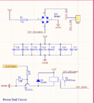
This picture is my full bridge schematic.

- - - Updated - - -

This picture is my 310V input schematic.
relay is for control 310V input.
 

Attachments

  • 42.png
    42.png
    57.6 KB · Views: 122
  • 46.png
    46.png
    39.5 KB · Views: 114

Hi Hadi,
I fully agree with the safety concerns Klaus raised :!:

Besides this, your board design doesn't look well. Too long traces, stubs etc.
There is a lot of chance for trace inductance & crosstalk, especially on the gate lines, but also on the power bridge.

I still see the 1k G-S resistors, and also additional Zener diodes?!? They will kill a defined Gate control. Remove them!

Snubbers are for dampening of ringing/oscillation, not for control of dI/dT. They should be placed over each Mosfet.
Snubbers depend on the trace/package inductance& D-S capacitance. A design duide can be found here.
Remove the Diodes D6/7/1´4/15 across Mosfets, they will only increase D-S capacitance. Mosfets already have builtin Body diodes.

Control of dV/dT will be done by Gate resistors, which will act as an RC lowpath, considering the G-S cap.
valid for all Mosfets: R9 should be increased to ~20R to make Ton slower. D4 should get an add. ~10R in series, to make also Toff slower (D4 without R will lead to fast Toff, resulting in high dV/dT)

R13/D13 to be removed, they are not needed.

Are your heatsinks isolated from Exposed pads of Mosfet? If not, they will have Drain voltage, and need to be isolated each to any other signal :!:

Overall, this gets analog, and without additional layout optimization & detailed simulation/measurement, circuit optimization gets impossible.
 
Last edited:
Thank you.
I will do your tips.
Do you have any things such as pdf or article .... about high voltage PCB layout? I want to learn.
My PCB is big because do several works.just right part of my PCB for full bridge circuit. I try that decrease gate lines and did it.
Lines are short and does not have any loop.
 

Hi,

Lines are short and does not have any loop.
I don't agree. Your wiring is not as short as it should be.

And every signal needs to be a loop.
Always think as signal path and it's return path.

Klaus
 

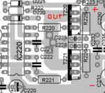
Only to give you an impression:
Halfbridge.PNG
It's IR2110 with two IRF4020
That's what I call an optimized layout.
 

If the mosfets are dead it is likely the driver ic's will be too ... buy a variac to allow the HVDC to come up slowly ...

- - - Updated - - -

Also try 220 ohm gate turn on resistors to limit dv/dt for starters until you gain confidence, if it works at 24VDC and not higher, dv/dt ( or di/dt) is always the issue ...

- - - Updated - - -

what frequency are you trying to switch at?

Hi
PWM frequency = 20 KHz

- - - Updated - - -

Only to give you an impression:
View attachment 147963
It's IR2110 with two IRF4020
That's what I call an optimized layout.

OK very good.
In my PCB distance is 76mm.
Does your circuit have snuber on mosfets?

- - - Updated - - -

Hi,


I don't agree. Your wiring is not as short as it should be.

And every signal needs to be a loop.
Always think as signal path and it's return path.

Klaus

Thank you.
Yes , you are right. lines are 76 mm.

- - - Updated - - -

Now I measure rise time and fall time.
Rise time (turning on mosfet time) = 180 nS (R gate(on) = 22 Ohm)
fall time (turning off mosfet time) = 90 nS (R gate(off) = 10 Ohm)
Is it good?
 
Last edited:

Does your circuit have snuber on mosfets?
Yes, thought you have seen them on the layout ;-) R/C225 and R/C226
Now I measure rise time and fall time.
Rise time (turning on mosfet time) = 180 nS (R gate(on) = 22 Ohm)
fall time (turning off mosfet time) = 90 nS (R gate(off) = 10 Ohm)
Is it good?
Still quite fast, but much better than before.
Consider IRFP460A specifies Absolute Maximum rating for Peak Diode Recovery dV/dt as 3,8V/ns (beyond, it will trigger bipolar latch-up, resulting in excessive short-circuit)
Your stage switches 300V, so min turn-on time has to be bigger than: (300/3,8)= 79ns.
So it seems you are above this.
If you want a higher safety margin for investigations, you may increase the R-values by approx. x2 to x5.
 

You are talking about the rise and fall time of the voltage? unfortunately long leads make good antenna's
 
Hi
I don't know their good value. In your opinion what are their value( rise and fall time)?
Several question:
1) Which is important Rise time or fall time or both?
2) should always be rise time more than fall time ( It means R gate ON bigger than R gate OFF)?why?
Thank you a lot for your answers.
Hadi dastour
 
Last edited:

1) Which is important Rise time or fall time or both?
2) should always be rise time more than fall time ( It means R gate ON bigger than R gate OFF)?why?
1.) t-on is most important due to Body Diode Recovery restrictions. See my last post.
2.) t-off should be faster than t-on to ensure break-before-make time.
Let's assume upper FET is closed, lower FET open. Then the upper should open (=toff) before the lower closes (=ton), and vice versa.Therefore you usually design toff shorter than ton.
But on the other hand, toff should not be too fast, as this will increase ringing (which then may not be dampened enough even with snubber).
So you see, it's finetuning & tradeoff of parameters due to different effects, and going to extremas of parameters is always a bad choice...
 
Let's assume upper FET is closed, lower FET open. Then the upper should open (=toff) before the lower closes (=ton), and vice versa.Therefore you usually design toff shorter than ton.
Can't agree. In bridge topologies you can not rely only in the "toff" and "ton" times, one needs to add additional dead time.

What you are suggesting is to turn the lower FET ON at the same time you turn the upper FET OFF i.e. apply control signals at the same time without any dead time and rely on the fact that you have tuned the "toff" and "ton" times correctly. That is playing with fire and therefore not a good practice. Dead-time is a must. Review standard literature.
:roll: I never said this ton-toff tailoring is sufficient to ensure break-before-make in any conditions...
It was more a basic explanation about reason for unsymmetrical ton/toff. Please consider the context.
I fully agree that in some setups (e.g. Hi-voltage, fast FET...) additional Dead-time may be needed.
 

A larger turn on resistor, 100 - 220 ohm and a smaller turn off resistor, ~47 ohm, will help with CURRENT rise and fall times and will help with dv/dt, and therefore help get you going with higher bus voltages... however layout is still VERY important ...

- - - Updated - - -

also the differing resistors will give you additional dead-time, however for prototype dead-time should be 1uS at least ...
 

Status
Not open for further replies.

Similar threads

Part and Inventory Search

Welcome to EDABoard.com

Sponsor

Back
Top