Continue to Site

Welcome to EDAboard.com

Welcome to our site! EDAboard.com is an international Electronics Discussion Forum focused on EDA software, circuits, schematics, books, theory, papers, asic, pld, 8051, DSP, Network, RF, Analog Design, PCB, Service Manuals... and a whole lot more! To participate you need to register. Registration is free. Click here to register now.

[SOLVED] CMOS Op-amp simulation.

Status
Not open for further replies.

sakkano2

Newbie level 4
Joined
Dec 18, 2017
Messages
5
Helped
0
Reputation
0
Reaction score
0
Trophy points
1
Activity points
58
Hello.
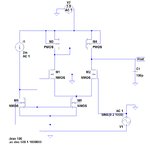
I need to design a single-phase Cmos op-amp as my homework.I try to design the circuit shown below and made calculations on it but when i simulate the circuit on LTSpice i get unwanted gain value.I try to make adjustements on Mosfet s to reach the desired gain of 20dB but i can not reach that value.Is there anything wrong with my circuit? and how can i reach 20dB gain. I will be very gratefull if you can help me.
My paramaters are;
Gain=20dB
Gain Bandwith = 1MHz
Supply Voltage = 2.5Volts
Power Budget=5mW
Load capacitance=100pF

I assume ICMR as -1 to 2 Volts , K'p =63uA , K'n=325uA , Vtp=-0.46V, Vtn=0.49.
With respect to these values i found W/L ratios and transconductance values.
cmosdesign1.png
cmosdesign.png


and my Spice file is:

Code dot - [expand]
1
2
3
4
5
6
7
8
9
10
11
12
13
14
15
16
17
M2 Vout 0 N005 0 NMOS l=5u w=3u ad=96e-12 as=96e-12 pd=44e-6 ps=44e-6 m=1 nrd=1.0 nrs=1.0
M1 N002 N003 N005 0 NMOS l=5u w=3u ad=96e-12 as=96e-12 pd=44e-6 ps=44e-6 m=1 nrd=1.0 nrs=1.0
M4 N001 N002 Vout N001 PMOS l=4u w=5u ad=96e-12 as=96e-12 pd=44e-6 ps=44e-6 m=1 nrd=1.0 nrs=1.0
M3 N001 N002 N002 N001 PMOS l=4u w=5u ad=96e-12 as=96e-12 pd=44e-6 ps=44e-6 m=1 nrd=1.0 nrs=1.0
M5 N005 N004 0 0 NMOS l=1u w=2u ad=96e-12 as=96e-12 pd=44e-6 ps=44e-6 m=1 nrd=1.0 nrs=1.0
M6 N004 N004 0 0 NMOS l=1u w=2u ad=96e-12 as=96e-12 pd=44e-6 ps=44e-6 m=1 nrd=1.0 nrs=1.0
C1 Vout 0 100p
I1 N001 N004 2m AC 1
V1 N003 0 SINE(0 2 1000) AC 1
V2 N001 0 2.5 AC 1
.model NMOS NMOS
.model PMOS PMOS
.lib C:\Users\Bugra\Documents\LTspiceXVII\lib\cmp\standard.mos
;tran 100
.ac dec 500 1 1000000
.backanno
.end


Thank you very much for your help.
Have a Good Day.
 
Last edited by a moderator:
Did you simulate the DC operating points of this circuit? I think your ICMR can't be negative, so it won't work with -1V input common mode voltage.
Your minimum input ICM voltage should be 2*Vtn+Vdsat5 ~ 1.1...1.2V, but absolutely not a negative value. Connect a 1.2V DC voltage source between the gnd and the AC1 source's negative pin.
I attach a link which helps: http://curtisma.org/wp-content/uploads/2014/01/Telescopic-Differential-Amplifier-Design.jpg
On the schematic the V4 source sets the DC input common mode voltage (set this to 1.2V).
V2 and V3 set the input differential mode voltages, for AC simulation only one of them is enough, you can replace the other one with a wire.
 
Last edited:
I assume ICMR as -1 to 2 Volts , K'p =63uA , K'n=325uA , Vtp=-0.46V, Vtn=0.49.

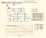
I also think a negative ICM voltage isn't possible with a simple OTA topology. However if your lower ICMR limit should reach close to GND, it would be better to use a p-channel input OTA. Find here a suggestion for such a p-OTA, simulated with your above model parameter values:

1stage-p-OTA_1MHz_100pF_ICMR.png

Its reasonable ICMR = 0.4 .. 1.6V .
 
Status
Not open for further replies.

Similar threads

Part and Inventory Search

Welcome to EDABoard.com

Sponsor

Back
Top