Continue to Site
Follow along with the video below to see how to install our site as a web app on your home screen.
Note: This feature may not be available in some browsers.


Hi,
I think, from the little I understand, the question is relative to several parameters not provided. What power can the LDO draw? That will affect the current source value.
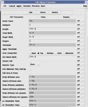
Vref is whatever you want it to be. R1 and R2 divide down V out to match Vref. R1 and R2 can be calculated from the formula in the little blue text box at the top right of the simulation screenshot. I hopew that's what you meant.
R load will depend on the power you give the LDO and its limitations. Aiming for 3.3V, I get ~3.295V with a 1k load in my simulation - it can output a feeble 3mA (the rest of the current drawn on VS1 is regulator operation). C load maybe has to do with stability, and I think I remember the larger the Cload the greater the stability, but the slower the response.
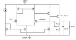
The screenshot is a simulation of a bog-standard regulator copied from a CMOS version - the other image attached. It's BJT's instead of CMOS design, but that's not really here nor there.
View attachment 142974 View attachment 142973
What you ask for are "design-to" application values for
the most part. Product definition. If nobody has these
for you then suggest you make up some stuff that is
credible.
Cload will be what makes output transient accuracy
"good enough" for the powered load (an active device
with its own attributes) on load-step events. Rload
(or Iload, depending on load behavior) has to assume
min and max levels. Vout, same deal. Pick a job, any
job, and all of this unfolds.