speedEC
Full Member level 6
Dear all,
I need to interface Silicon Labs Si4432 v1.0 Module with PIC16F1938 thru' SPI module. I could not able to receive signal from Si4432.
The settings are follows:
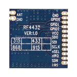
Si4432 V1.0 RF MODULE: SILICON LABS
MCU - PIC16F1938 - 8 BIT MCU
HARDW(A)IRES CONNECTION:
GND - GND
GPIO_0 - 0 V - UNCONNECTED TO MCU
GPIO_1 - 2.90 V - UNCONNECTED TO MCU
GPIO_2 - 1.42 V - UNCONNECTED TO MCU
VDD - 2.90V (2 AA BATTERY)
SDO - 0V - CONNECTED TO MCU'S SDI
SDI - 0V - CONNECTED TO MCU'S SDO
SCLK - 0V - CONNECTED TO MCU'S SCLK
nSEL - 0V - CONNECTED TO MCU'S DIG I/O PIN
nIRQ - 0V - CONNECTED TO MCU'S INTERRUPT PIN
SDN - GND - Always ON
GND - GND
MCU:
1. RB0 - SET AS INPUT (TRISB0 = 1) for nIRQ interrupt
2. RC4 - SET AS INPUT (TRISC4 = 1) for SDI
3. MCU internal clock - 4 MHz
4. INTIE and SSPIE interrupts enabled and GIE set
SW CODE:
init SPI Module:
Reading Si4432:
1. char ItStatus1;
2. ItStatus1 = SpiReadRegister(0x03); //read the Interrupt Status1 register
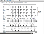
Si4432 - Serial Peripheral Interface (SPI)
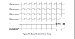
The Si4430/31/32 communicates with the host MCU over a standard 3-wire SPI interface: SCLK, SDI, and nSEL. The host MCU can read data from the device on the SDO output pin. A SPI transaction is a 16-bit sequence which consists of a Read-Write (R/W) select bit, followed by a 7-bit address field (ADDR), and an 8-bit data field (DATA) as demonstrated in Figure 3. The 7-bit address field is used to select one of the 128, 8-bit control registers. The R/W select bit determines whether the SPI transaction is a read or write transaction. If R/W = 1 it signifies a WRITE transaction, while R/W = 0 signifies a READ transaction. The contents (ADDR or DATA) are latched into the Si4430/31/32 every eight clock cycles. The timing parameters for the SPI interface are shown in Table 10. The SCLK rate is flexible with a maximum rate of 10 MHz.
any help?
thanks
pmk
I need to interface Silicon Labs Si4432 v1.0 Module with PIC16F1938 thru' SPI module. I could not able to receive signal from Si4432.
The settings are follows:
Si4432 V1.0 RF MODULE: SILICON LABS
MCU - PIC16F1938 - 8 BIT MCU
HARDW(A)IRES CONNECTION:
GND - GND
GPIO_0 - 0 V - UNCONNECTED TO MCU
GPIO_1 - 2.90 V - UNCONNECTED TO MCU
GPIO_2 - 1.42 V - UNCONNECTED TO MCU
VDD - 2.90V (2 AA BATTERY)
SDO - 0V - CONNECTED TO MCU'S SDI
SDI - 0V - CONNECTED TO MCU'S SDO
SCLK - 0V - CONNECTED TO MCU'S SCLK
nSEL - 0V - CONNECTED TO MCU'S DIG I/O PIN
nIRQ - 0V - CONNECTED TO MCU'S INTERRUPT PIN
SDN - GND - Always ON
GND - GND
MCU:
1. RB0 - SET AS INPUT (TRISB0 = 1) for nIRQ interrupt
2. RC4 - SET AS INPUT (TRISC4 = 1) for SDI
3. MCU internal clock - 4 MHz
4. INTIE and SSPIE interrupts enabled and GIE set
SW CODE:
init SPI Module:
Code C - [expand]
Reading Si4432:
1. char ItStatus1;
2. ItStatus1 = SpiReadRegister(0x03); //read the Interrupt Status1 register
Code C - [expand]
Si4432 - Serial Peripheral Interface (SPI)
The Si4430/31/32 communicates with the host MCU over a standard 3-wire SPI interface: SCLK, SDI, and nSEL. The host MCU can read data from the device on the SDO output pin. A SPI transaction is a 16-bit sequence which consists of a Read-Write (R/W) select bit, followed by a 7-bit address field (ADDR), and an 8-bit data field (DATA) as demonstrated in Figure 3. The 7-bit address field is used to select one of the 128, 8-bit control registers. The R/W select bit determines whether the SPI transaction is a read or write transaction. If R/W = 1 it signifies a WRITE transaction, while R/W = 0 signifies a READ transaction. The contents (ADDR or DATA) are latched into the Si4430/31/32 every eight clock cycles. The timing parameters for the SPI interface are shown in Table 10. The SCLK rate is flexible with a maximum rate of 10 MHz.
any help?
thanks
pmk