Continue to Site

Welcome to EDAboard.com

Welcome to our site! EDAboard.com is an international Electronics Discussion Forum focused on EDA software, circuits, schematics, books, theory, papers, asic, pld, 8051, DSP, Network, RF, Analog Design, PCB, Service Manuals... and a whole lot more! To participate you need to register. Registration is free. Click here to register now.

How to Plot transconductance Vs Vid(diffrential) at fully differential OTA in ADS

Status
Not open for further replies.

shimaa.heydari

Junior Member level 1
Joined
Oct 21, 2017
Messages
16
Helped
0
Reputation
0
Reaction score
0
Trophy points
1
Activity points
158
Hi every body
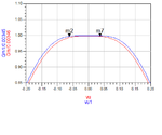
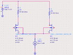
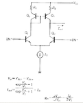
I have an OTA with differential input and fully differential output. please help me how can i see the correct Gm curve of ota Vs differential input voltage. I want a simulation such this picture that is reported in many papers. I dont know:
1- how connect the source (DC or AC?) of input to Gate terminales of two input mosfets?
2- I have two node for output. now what i must connect to this nodes to see Gm curve?
Thank you.
 

Attachments

  • Gm-Vd.png
    Gm-Vd.png
    8.5 KB · Views: 194
  • ota.png
    ota.png
    12.5 KB · Views: 211

1- how connect the source (DC or AC?) of input to Gate terminales of two input mosfets?
DC Voltage source with inverse polarity.

2- I have two node for output.
now what i must connect to this nodes to see Gm curve?
Insert Current Probe between resistor and drain.

Simply plot Gm based on your definition of Gm.
 
Last edited:

thank you pancho_hideboo for your good response.

1- you mean that i use two DC voltage? put a Dc supply in Gate of M1 and another DC supply with opposite polarity in Gate of M2?
2- is it true that i put a resistor between drain of M1(vo1) and drain of M2(vo2)? and now use the current of this resistor for plot Gm=iout/vid? because i want fully differential output.
3- how must be the value of this resistor? is it important in accuracy of Gm curve?

i need to your help..
please attend me..
 

Attachments

  • ota.png
    ota.png
    12.5 KB · Views: 129

1- you mean that i use two DC voltage? put a Dc supply in Gate of M1 and another DC supply with opposite polarity in Gate of M2?
Yes.

2- is it true that i put a resistor between drain of M1(vo1) and drain of M2(vo2)?
I can not understand what you want to mean at all.

and now use the current of this resistor for plot Gm=iout/vid?
Yes.
So insert current probe between resistor and drain.

3- how must be the value of this resistor?
is it important in accuracy of Gm curve?
No.
It determine voltage of drain.
If drain current large, MOSFET will be in triode region.
 

pancho_hideboo! your guidances are very useful for me :clap:.

about the n.2 question:
are you think I put a resistance between output mosfet Drain and ground?
No..!
i have a fully differential OTA ok?
thus I have two drain. one drain is Vout1 and another is Vout2.
now i put a resistance between this two drain. because i want fully differential output.
this resistant be considered as a load for OTA. and it's different values give me different Gm curevs..!!
I use the current probe in series of this resistance. my work is wrong?
 

Transconductance is defined for shorted output. Shorting Vout1 and Vout2 with a current probe is the appropriate way to measure conductance.
 
thanks a lot Dear pancho_hideboo and FvM.

with your helps finally I could plot my desirable curve. i explain this in ADS for other friends:

1- we must use two DC voltage. put a DC supply in Gate of M1 and another DC supply with opposite polarity in Gate of M2. (M1 & M2 are differential inputs)
2- Short Vout1 and Vout2 with a current probe. (Vout1 & Vout2 are differential outputs)
3- sweep the Vdc(magnitude of M1 & M2) by simulation DC in ADS (for example:-0.6 to +0.6)
4- name or label vip for Gate of M1 and vin for Gate of M2
5- Run the the simulate.
6- in graphic window make two equation: (vid=vip-vin & Gm=i prob/vid) that i prob is the current prob in stage.2.
7. plot Gm vs vid.
enjoy your discovery.. ! :clap:;-)
 

Attachments

  • 5.png
    5.png
    35.3 KB · Views: 237

Transconductance is defined for shorted output.
Shorting Vout1 and Vout2 with a current probe is the appropriate way to measure conductance.
I don't think so.

6- in graphic window make two equation: (vid=vip-vin & Gm=i prob/vid) that i prob is the current prob in stage.2.
Wrong.
First, your gate voltage is not appropriate.
Second, can you understand Gm ?
Gm is a derivative.
 

Attachments

  • 2017-1023-1135-24.png
    2017-1023-1135-24.png
    81.7 KB · Views: 194
  • 2017-1023-1133-29.png
    2017-1023-1133-29.png
    115 KB · Views: 157
  • 171023-205356.png
    171023-205356.png
    11.2 KB · Views: 140
Last edited:

I don't think so.

Wrong.
First, your gate voltage is not appropriate.
Second, can you understand Gm ?
Gm is a derivative.

Why wrong? :-(
- I want plot the Gm of hole OTA. my OTA has 8 mosfet.
- Gm is the Gain of transconductance= iout/Vid.
- Vid is the different between input gates voltage of mosfet. and iout is the current passing from the two nodes of output mosfets. (fully differential output)
- plotting Gm vs Vid tell me the linearity rang of my OTA is good or not. this show me the safe range of input that OTA works correct and how much the nonlinearity affected on OTA's Work.

if you have another defination for this case of curve that i need, please explain step by step and very very simple.
 

- Gm is the Gain of transconductance= iout/Vid.
Wrong.
Surely learn very basic things.
Gm is d(iout)/d(Vid).

Again surely learn very basic things.

if you have another defination for this case of curve that i need, please explain step by step and.
Surely see my figures which are ADS schematic and results, where I did DC and AC Analyses.

Your gate voltages are minus values.
Do you think such gate voltages have any meaning ?

Again surely learn very basic things.
 
Last edited:

wooooo..

you learn me very thinks pancho_hideboo ..
yes i am wrong. thank you for inform me and for your important time to guide me.
but a problem..

* in your picture that the transistores are bipolar, The OTA is single ended.
* in picture that you draw in ADS window the OTA is fully differential. you believe that also for differential output we must subtract the current of two mosfet?
with No shorting output nodes and No load putting between output nodes and No measuering the current of this load?

i want to know. you are my teacher..
 

enjoy your discovery.. ! :clap:;-)
No one can enjoy your very wrong explanations.

* in your picture that the transistores are bipolar, The OTA is single ended.
There is no difference between BipBJT and MOSFET.

I mean current difference should be evaluated with actual load condition.
Here single ended current output is a difference between Id1 and Id2.

* in picture that you draw in ADS window the OTA is fully differential.
you believe that also for differential output we must subtract the current of two mosfet?
Yes.
Current difference should be evaluated with actual load condition.

with No shorting output nodes
Yes.

and No load putting between output nodes
and No measuering the current of this load?
No.
Current difference should be evaluated with actual load condition.
 
Last edited:

Vg1 = Vcom + Vdiff/2
Vg2 = Vcom - Vdiff/2

Vcom = (Vg1 + Vg2) / 2
Vdiff = Vg1 - Vg2

Id1 = Icom/2 + Idiff
Id2 = Icom/2 - Idiff

Icom = Id1 + Id2
Idiff = (Id1 - Id2) / 2

Gm_com_diff = d(Icom) / d(Vdiff)
Gm_diff_Diff = d(Idiff) / d(Vdiff)

Your current probe makes two drains short.
So drain voltages are same value regardless of Vdiff value.
This can not reflect actual operation of MOSFETs.

We can not measure Icom, if current probe is inserted like your test bench..
 

Status
Not open for further replies.

Similar threads

Part and Inventory Search

Welcome to EDABoard.com

Sponsor

Back
Top