abouabdelmajid
Newbie level 5
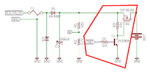
Hi everyone.Here is a a circuit showing how a "PWM Solar Charge controler" works. the principal work of this controler is using arduino's PWM to switch on the transistor 2N3904 to let the 12V battery absorb the energy from the solar pannel when the voltage of the solar pannel is under the actual battery's voltage and in an opposite situation the transistor should be switched off. so using the mosfet driver (wich is in the middle of red circle) is an important thing but i still dont know how it works ?!
after many researches i found that the driver is there to provide the current and also drives the gate with an appropriate voltage level not high to avoid the risk of damaging the mosfet but also high enough to produce a low Rdson. But my question is how it works ?!! when the transistor 2N3904 is switched on where the curent goes ? why do we need the mosfet IRF95530 ? to amplify the voltage ? but how the current get into the mosfet ? can anybody tell me how the Mofset driver work ?!!
after many researches i found that the driver is there to provide the current and also drives the gate with an appropriate voltage level not high to avoid the risk of damaging the mosfet but also high enough to produce a low Rdson. But my question is how it works ?!! when the transistor 2N3904 is switched on where the curent goes ? why do we need the mosfet IRF95530 ? to amplify the voltage ? but how the current get into the mosfet ? can anybody tell me how the Mofset driver work ?!!