Continue to Site

Welcome to EDAboard.com

Welcome to our site! EDAboard.com is an international Electronics Discussion Forum focused on EDA software, circuits, schematics, books, theory, papers, asic, pld, 8051, DSP, Network, RF, Analog Design, PCB, Service Manuals... and a whole lot more! To participate you need to register. Registration is free. Click here to register now.

power consumption in 2-bit multiplexer

Status
Not open for further replies.

milad71

Newbie level 3
Joined
Jun 14, 2017
Messages
4
Helped
0
Reputation
0
Reaction score
0
Trophy points
1
Activity points
22
dear friends
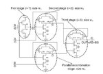
i want to calculate power consumption in multiplexer but i dont konw how to choose the inputs (a , b and s) to evaluate exact power?
the output of multiplexer is o=A*(snot)+B*S .
please guide me
 

Are you trying to calculate the power consumption of a physical circuit or is this more of a theoretical practice? The inputs are all high impedance so I don't see why the input settings would affect the overall power consumption. The circuit/IC should have some supply current and the power consumption is simply supply voltage * supply current. I guess if you were planning on sourcing or sinking current to the output you would want to set the inputs such that the output current is maximized and then take your current reading.
 

Within the mux you have on resistance of the switches
and shunt capacitances. Input shunt cap causes loss in
the driving network's resistance. Output shunt cap loss
is across Ron. You should have minimal, but maybe not
negligible, losses through the FET gates' capacitances,
to the internal gate drivers' on resistance, to the supplies.
Through-losses will be across Ron through the load C
(if this is CMOS logic) or perhaps also some DC losses if
driving a resistive impedance).

Of course you also have CVf current in the enable paths
if toggling.

You should try to understand the structure, draw it out
and the loss paths should become pretty evident to
inspection. Old CMOS databooks from RCA, et al have
nice detailed transistor level schematics which you
could simplify for analysis purposes, to Rs and Cs.
 

1.JPG

it is a physical circuit, in proposed paper is not any information about a and b and when i change this inputs (a and b) i have different power consumption. i know how to calculate the power but i dont know,how should we select inputs?
 

it is a CMOS logic. my problem is not a theoretical definition and i know about basic definitions. my issue is in hspice simulation. also I read your describtion but i did not understand what do you mean ?!

- - - Updated - - -

Are you trying to calculate the power consumption of a physical circuit or is this more of a theoretical practice? The inputs are all high impedance so I don't see why the input settings would affect the overall power consumption. The circuit/IC should have some supply current and the power consumption is simply supply voltage * supply current. I guess if you were planning on sourcing or sinking current to the output you would want to set the inputs such that the output current is maximized and then take your current reading.

:!: please tell me more about inputs selection.
 

If the MOSFETs have finite "off" leakage, the logic state
of each gate will modulate DC supply current.

IDDQ testing takes this a step further, criticizing supply
current changes as you step through a truth table, to
look for defects that are short of functional failure but
not as-intended.
 

Status
Not open for further replies.

Part and Inventory Search

Welcome to EDABoard.com

Sponsor

Back
Top