Continue to Site

Welcome to EDAboard.com

Welcome to our site! EDAboard.com is an international Electronics Discussion Forum focused on EDA software, circuits, schematics, books, theory, papers, asic, pld, 8051, DSP, Network, RF, Analog Design, PCB, Service Manuals... and a whole lot more! To participate you need to register. Registration is free. Click here to register now.

Via hole vs. Ground in ADS

Status
Not open for further replies.

laperla

Full Member level 4
Joined
Oct 17, 2009
Messages
191
Helped
2
Reputation
4
Reaction score
3
Trophy points
1,298
Activity points
2,364
Dear friends
I have problem with via in ADS
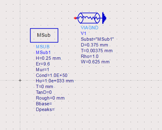
I have layout in Momentum I transfer it to schematic page and use a ground
but when I use via hole in momentum page instead of ground in schematic, the result doesn't be same
Via hole isn't ground?
 

If the frequency is too high VIAs can not be considered tied to GND anymore.They will affect the frequency response.
 
the frequency range is 1-4GHz.
How can I define via as ground in this frequency?
 

Your question is not clear.

Via in Momentum (and in reality) has physical size, and this results in inductance + resistance. Ideal ground in schematic does not exist in reality, so some small difference is expected.

If you have large difference, perhaps something is wrong with your model. Check if your via in Momentum really connects to ground. One possible check is to see what DC resistance to ground you have in that path.

To make a via to ground in Momentum, you need to draw something on a layer (for example hole layer) and that layer must be included in the Momentum substrate as a via, connecting to infinite ground boundary.

via.PNG
 
Last edited:
This is the definition of layer in momentum

Untitled.png
 

Substrate looks ok. So what difference do you see? Screenshot or data, please.
 
S21 response shows in fig.
pink line is the filter with via hole others with ground
S21.png
 

Obviously, a via involves some series inductance and thus doesn't behave identical to massive ground. You can try an array of multiple vias.

- - - Updated - - -

It's not completely clear which geometries are you comparing.
 
I sweep diameter of hole but s21 didn't change
 

I sweep diameter of hole but s21 didn't change

The "real" via in Momentum has some length, the schematic ground is an ideal short.
You can get more realistic ground in schematic simulation by using via model in schematic (instead of ideal short).


Depending on where you place the via, current flow in Momentum (and reality) will change. This is why EM results are more accurate than cascading schematic models.

pin_on_edge.png


explicit_line_pin_on_edge.png
 

In the schematic page, the filter has dc voltages for tuning the varactors. I want to connect some varactors to GND
Should I connect ground of dc sources to ac sources? I mean the ground of varactors is different from ground of via hole?
 

In the schematic page, the filter has dc voltages for tuning the varactors. I want to connect some varactors to GND
Should I connect ground of dc sources to ac sources? I mean the ground of varactors is different from ground of via hole?

To my understanding you have a DC voltage to tune the varactors in a filter structure right ?? And you have-probably-done a EM simulation with a starting frequency not from 0 Hz and therefore you cannot see the effect of varactors even you apply a DC voltage.
If I have correctly understood your problem and if the case is that, I suggest you do the simulation from 0 Hz using with Momentum Microwave mode.
 
I have a filter in Momentum page. I should transfer layout from Momentum to Schematic page for connecting varactors. I don't do simulation in Momentum page I do it in Schematic. For tuning varactors, I need to bias voltage sources like attached figure
2.png

- - - Updated - - -

I use multiple via for reducing the effect of via's inductors
 
Last edited:

I should transfer layout from Momentum to Schematic page for connecting varactors. I don't do simulation in Momentum page I do it in Schematic.

We need to guess again, because your information is not complete.

So your via subcircuits have an emModel with valid data from Momentum? If done properly, the "layout" via blocks that you show connect to ground (same as schematic ground). Test that: test circuit with via block connected to a schematic port and check S11.

For the Momentum setup, Bigboss is right: you need to specify 0 Hz lower frequency. For this small layout with 4 vias, Momentum RF mode or Microwave mode are both ok.

Besides these details, I think that splitting layout into such small pieces will be much less accurate than "full" EM models of larger layout sections, but that's another topic.
 
For the Momentum setup, Bigboss is right: you need to specify 0 Hz lower frequency. For this small layout with 4 vias, Momentum RF mode or Microwave mode are both ok.

Volker,

Is that correct ?? I have simulated many structures in RF mode with 0Hz lowest frequency but I have seen many times convergence errors in schematic simulations using with especially HB.
RF mode does not takes the lowest frequency as 0Hz, it takes very close to DC but not 0Hz.That's my observation.
 
I simulate circuit with via block and ground
S11 and S21 frequency response is related to circuit with ground
S33 and S43 is related to circuit connected to Via block
4.png5.png6.png

Also, I do simulation from 0Hz in Schematic and Momentum
 

In dc annotation shows that via hole is not 0 V.
7.png
 

RF mode does not takes the lowest frequency as 0Hz, it takes very close to DC but not 0Hz.That's my observation.

My understanding: Momentum RF mode can go down to DC, whereas Microwave mode only works at "higher" frequencies. If you specify 0 Hz in Microwave mode, this switches to RF mode at low frequency behind the scenes.

But I must admit that I use Momentum RF mode down to DC all the time, without actually using results myself in HB. My own DC results look perfectly fine. I think there is another mistake in laperlas setup.

- - - Updated - - -

In dc annotation shows that via hole is not 0 V.

Then there is a mistake/problem in your setup somewhere.
Again: Create a testbench with just via block and port, and show the S11 (low frequency and DC) into the via block.

25nV.PNGView attachment via_gnd_wrk.zip


Can you upload the archived workspace, reduced to this one design, so that we have a chance to see what you did?
 
Last edited:

I did simulation according to below figures


8.png9.png10.png


S33 and S43 is related to the Via hole
S77 and S87 is related to the ideal ground
Is it true?
 

Status
Not open for further replies.

Part and Inventory Search

Welcome to EDABoard.com

Sponsor

Back
Top