Continue to Site

Welcome to EDAboard.com

Welcome to our site! EDAboard.com is an international Electronics Discussion Forum focused on EDA software, circuits, schematics, books, theory, papers, asic, pld, 8051, DSP, Network, RF, Analog Design, PCB, Service Manuals... and a whole lot more! To participate you need to register. Registration is free. Click here to register now.

convert 1Mhz square wave pwm (5v and Gnd) to 1 Mhz square wave (+20v and -20v)

Status
Not open for further replies.

edobp

Newbie level 4
Joined
Jun 8, 2017
Messages
5
Helped
0
Reputation
0
Reaction score
0
Trophy points
1
Activity points
40
hello all.
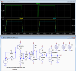
im planning to convert 1mhz pwm from a microcontroller (5v and gnd) to a positive and negative (+20v and -20v) pwm (1mhz). I already did this by using a bjt transistor (bd139 and bd140), please see the pict below.

ivGHT.png

the circuit above works to convert the (+5v/gnd) pwm to (+20v/-20v) pwm with 100 kHz frequency. but when i raised the frequency to 1mhz the output was gone missing (drop to 0v). could anyone help me to get the solution of my problem? sorry if my explanation is pretty confusing, but it understanable, thank you.
 

Where are the Base Voltages of the output transistor ?? At least, there should be 2 diodes in series for a proper biasing.
 

What is the maximum output load current?

- - - Updated - - -

Where are the Base Voltages of the output transistor ?? At least, there should be 2 diodes in series for a proper biasing.
That's only really needed for an analog output to minimize crossover distortion.
It's not needed for a digital out, which the TS wants.
 

After simulating the circuit, the problem is the saturation delay of the BJT transistors.
Below is the simulation with modifications to reduce this delay.
I added speedup capacitors at the bases along with a Schottky clamp on Q1 to prevent its saturating.
Also changed Q4 to a faster transistor.

Why do you need such a fast PWM signal?
Capture.PNG
 
  • Like
Reactions: edobp

    edobp

    Points: 2
    Helpful Answer Positive Rating
What is the maximum output load current?

- - - Updated - - -

sorry i forgot to mention the current, actually the current i need is around 1-1,5 amps
 

thank you so much for the reply sir. i need the fast pwm signal to trigger an ultrasonic transducer for my thesis. the trigger voltage must be a pwm (positive and negative) with around +20 and -20v voltage, not to mention that the current needs is around 1 - 1,5amps.
 

sorry i forgot to mention the current, actually the current i need is around 1-1,5 amps
Then you'll need larger transistors or an added buffer stage since the devices you show are only good to 0.2A maximum.
 

Attachments

  • Capture.PNG
    Capture.PNG
    31.1 KB · Views: 107
Last edited:

Then you'll need larger transistors since the devices you show are only good to 0.2A maximum.

like TIP3055 series? is it also work with the circuit you posted above sir?
 

Hi,

thank you so much for the reply sir. i need the fast pwm signal to trigger an ultrasonic transducer for my thesis. the trigger voltage must be a pwm (positive and negative) with around +20 and -20v voltage, not to mention that the current needs is around 1 - 1,5amps.

Afaik ultrasonic transducers don´t need DC-free (symmetric) drive voltage.

Maybe it´s more simple to use a half bridge (there are ready to buy single IC solutions), or a full bridge.

Klaus
 

Hi,


Afaik ultrasonic transducers don´t need DC-free (symmetric) drive voltage.

Maybe it´s more simple to use a half bridge (there are ready to buy single IC solutions), or a full bridge.

Klaus

thank you so much for the reference sir. i will surely think about it.
 

Here's the LTspice simulation of a circuit with a MOSFET output that will drive a 1.5A peak load at ±20V into the load @ 1MHz.
It uses a MOSFET half-bridge driver with a bootstrap high-side output to control two N-MOSFETs supplied by 40V to generate a 0-40V output.
A capacitor blocks the output offset to give ±20V to the load. If the load is a capacitive transducer then the output capacitor may not be needed.

The cross-coupled NAND gates at the input generate two non-overlapping signals for the high and low MOSFETs to avoid high feedthrough current during the switching time.

N-MOSFETs other than shown on the simulation can be used but to get proper switching times and minimize power dissipation in the MOSFETs, they must have a low gate charge, as shown in their data sheet.
It should be below 20nC, (below 10nC would be better) with an ON resistance ≦0.1Ω, and a voltage rating of 60V or higher.

Capture.PNG
 

Status
Not open for further replies.

Similar threads

Part and Inventory Search

Welcome to EDABoard.com

Sponsor

Back
Top