Continue to Site

Welcome to EDAboard.com

Welcome to our site! EDAboard.com is an international Electronics Discussion Forum focused on EDA software, circuits, schematics, books, theory, papers, asic, pld, 8051, DSP, Network, RF, Analog Design, PCB, Service Manuals... and a whole lot more! To participate you need to register. Registration is free. Click here to register now.

Layout Pattern for Vertical SMA Connector

Status
Not open for further replies.

pancho_hideboo

Advanced Member level 5
Joined
Oct 21, 2006
Messages
2,847
Helped
767
Reputation
1,536
Reaction score
733
Trophy points
1,393
Location
Real Homeless
Activity points
17,490
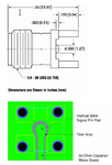
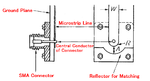
I want to use vertical type SMA(=Straddle Type) Connector on two layers PCB.

What layout patterns are recommended for Ground Plane and Signal Plane ?

Attached figures for Coplanar line and Microstrip line.
 

Attachments

  • Coplanar.png
    Coplanar.png
    82.3 KB · Views: 148
  • Microstrip.png
    Microstrip.png
    49.9 KB · Views: 139
Last edited:

the abrupt right angle will incur a series inductance. And the proximity of the ground plane will cause a parasitic shunt capacitance. So you model it like a lumped element lowpass filter with a series inductor and shunt capacitors, and vary the capacitance so the VSWR is low and the lowpass cutoff frequency is higher than your band of operation. That dimension A can be varied to add or subtract capacitance to achieve the above.

Sorry I do not have actual physical dimensions to suggest though. maybe the manufacturer can suggest some?
 

This is another example for two layers PCB.
Cyan and Orange : L1 Plane
Green : L2 Plane

RF signal line composes CPW(Coplanar Waveguide) with ground plane.
But it is very short line.
 

Attachments

  • 170506-211402.png
    170506-211402.png
    13.4 KB · Views: 156

Status
Not open for further replies.

Part and Inventory Search

Welcome to EDABoard.com

Sponsor

Back
Top