Continue to Site

Welcome to EDAboard.com

Welcome to our site! EDAboard.com is an international Electronics Discussion Forum focused on EDA software, circuits, schematics, books, theory, papers, asic, pld, 8051, DSP, Network, RF, Analog Design, PCB, Service Manuals... and a whole lot more! To participate you need to register. Registration is free. Click here to register now.

[SOLVED] Equations for regulator series pass

Status
Not open for further replies.

Seeker_IN

Newbie level 5
Joined
Feb 28, 2017
Messages
9
Helped
0
Reputation
0
Reaction score
0
Trophy points
1
Activity points
96
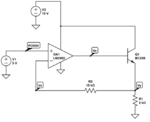
I have been trying to analyse the attached circuit. the equations which I write seems not to converge when I put in Mathcad. Below are the equations which I have for the circuit

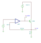
for the node Vy, (Vy-Vx)/R2+(Vy/R1)-Ic_Q1=0;

V2-Vce-Vy=0;

Vo-Vbe-Vy=0;

Vo=(POS5v-Vx+Voffset_OA1)*Avd;

Finally I need to get transfer function for Vy.

Please let me know where I am going wrong or what I am missing. Thanks
 

Attachments

  • Capture.PNG
    Capture.PNG
    36.4 KB · Views: 128

what parameter you want to compute for the regulator ?

one node equation and three loop equations . Any reason ?
 

I want to get the basic transfer function for Vy.
So, I just started putting the equations.
Later on I would add the temperature effects once the transfer function is obtained.
 

Why do you need equations and math for the simple circuit that has a voltage gain of only 1? Its output voltage is the same as its input voltage: +5V. Its R2 does nothing and can be replaced by a piece of wire.
 

Here is Vo taking account beta, Rbase and Vbe.

Vo :=(beta*R1+R1+Rb)/(beta*R1+R1)*V1+Vbe;
 

Here is Vo taking account beta, Rbase and Vbe.

Vo :=(beta*R1+R1+Rb)/(beta*R1+R1)*V1+Vbe;
No. Beta, the value of R1 and Vbe do not matter since the opamp controls the output voltage if the transistor is within its current ratings.
 

The equation defines the opamp output (Vo), not Vy. Refer to original diagram by member.
 

Attachments

  • DC_sol.png
    DC_sol.png
    8 KB · Views: 111

Why do you need equations and math for the simple circuit that has a voltage gain of only 1? Its output voltage is the same as its input voltage: +5V. Its R2 does nothing and can be replaced by a piece of wire.

G=1 is not completely true. The current flowing in the emitter of the transistor increses as R1 becomes low. This means that, depending on the beta of the transistor and its base resistance, the gain of the circuit will start to decrease as the R1 is lower than a minimum value that can be calculated from base resistance and beta. This because the base current multiplied by the beta will not be high enough to have a voltage across R1 equal to the input voltage.
As you said R2 is pratically useless.
 

The circuit shown has an input and output voltage of 5V and a load of only 2k so its output current is 2.5mA. Any little transistor, even one connected backwards will work in that circuit. The transistor can even be a diode or a piece of wire.
 

The circuit shown has an input and output voltage of 5V and a load of only 2k so its output current is 2.5mA. Any little transistor, even one connected backwards will work in that circuit. The transistor can even be a diode or a piece of wire.

Yes, of course. But if a more general analysis is required then beta and Rbase matter. This is the case if you want drive a quite "heavy" load. In this case you'll need to know how much heavy can be the load to be driven properly. If the values are that shown Q1 is pratically useless (as you already said).
 

Thanks for your insight on the Rbase and beta.
this circuit actually provides ADC reference voltage and at Vy node the actual max load is 20mA.
After writing the equations interms of Vbe and Vy(basically replaced Vo part) I was able to get convergence in Mathcad.

As it is stated R2 is useless, I also feel the same. If you could shed some light on why it would have been put in the first place then?
 

In real circuit, you don't have an ideal generator connected to the inverting input of the op-amp, but instead a generator with a given output impedance (Rgen). I think R2 has been inserted to compensate the effects of the input offset current of the op-amp. The current flowing through the Rgen will cause a voltage superimposed to that of the generator itself. Inserting R2, the current will cause a voltage that will be summed with opposite sign. This means if R2 = Rgen the effect of the current offset will be ideally cancelled.
However in practice you can avoid to insert R2.
 
Status
Not open for further replies.

Similar threads

Part and Inventory Search

Welcome to EDABoard.com

Sponsor

Back
Top