Continue to Site

Welcome to EDAboard.com

Welcome to our site! EDAboard.com is an international Electronics Discussion Forum focused on EDA software, circuits, schematics, books, theory, papers, asic, pld, 8051, DSP, Network, RF, Analog Design, PCB, Service Manuals... and a whole lot more! To participate you need to register. Registration is free. Click here to register now.

Broadside Coupled Balun ADS Port Definition

Status
Not open for further replies.

zangcn

Newbie level 3
Joined
Feb 14, 2017
Messages
3
Helped
0
Reputation
0
Reaction score
0
Trophy points
1
Activity points
34
Hello,

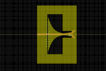
I am currently trying to simulate an output balun for a power amplifier with ADS Momentum. I am having trouble with some ports for the DC-blocking capacitors though. I set up the simulation with a finite ground plane and want to simulate with ports for the blocking caps on both the ground plane and the microstrip line on the unbalanced side of the balun. I defined the ports as differential ports but the log tells me there is a problem at higher frequencies (distance of the pins electrically large). I do know that I normally can define GND reference pins for each pin. However in this certain case what is the best way to define the ports as I do have caps on both sides?
 

Attachments

  • balun.png
    balun.png
    22 KB · Views: 99

First, you can not use any passive/active component in ADS Momentum EM simulations
Second, what is your intention to use finite ground underneath of the structure ?? Will it be covered by any GND environment ?? ?? Why not infinite ground ??
Third, there are many "close-in" ports, have you ever select calibration mode well ??
If the thickness of the substrate is larger than 1/10 lambda, Momentum will not like it.
There are other consideration too but I suggest you to read carefully Momentum help and if you can find, read some tutorials about it.
 

I need finitite ground as it is part of the balun. The design is for a Push-Pull PA. The two microstrip line on the right side of the image will be the connections to the drain pins of the transistors and to the left there is the unbalanced output. There will be a cooling block underneatch the amplifier but the part underneath the balun will be cut out. I am not trying to simulate the caps with momentum but want to simulate the structure for Cosimulation with the final design, so I need the ports where the DC-blocking caps will be connected. Calibration mode is set to "none". substrate is 0.508mm with an epr of 3.55. Without the ports for the caps there is no problem. However need to simulate the ports, I just dont know how?
 

I need finitite ground as it is part of the balun. The design is for a Push-Pull PA. The two microstrip line on the right side of the image will be the connections to the drain pins of the transistors and to the left there is the unbalanced output. There will be a cooling block underneatch the amplifier but the part underneath the balun will be cut out. I am not trying to simulate the caps with momentum but want to simulate the structure for Cosimulation with the final design, so I need the ports where the DC-blocking caps will be connected. Calibration mode is set to "none". substrate is 0.508mm with an epr of 3.55. Without the ports for the caps there is no problem. However need to simulate the ports, I just dont know how?
What is your max. frequency ?? Have you ever tried to make the calibration mode "SMD" ?? ( I guess that you use ADS2011 or newer )
 

Hi,
since I want to simulate the S-parameters of the balun later inside a harmonic balance simulation, my max. freq. is 20 GHz (5th harmonic of 4 Ghz, Design frequency 1-4 GHz).
I tried SMD calibration but it does not work in this case because you can not place several SMD-calibrated ports on the same edge of a structure. At least that is what ADS tells me.
Send me your project file as zap format, let me check what is wrong.
 

You can also try SMD or delta Gap port type then make it diffrential in Schematic simulation if needed.
 

Status
Not open for further replies.

Part and Inventory Search

Welcome to EDABoard.com

Sponsor

Back
Top