Continue to Site

Welcome to EDAboard.com

Welcome to our site! EDAboard.com is an international Electronics Discussion Forum focused on EDA software, circuits, schematics, books, theory, papers, asic, pld, 8051, DSP, Network, RF, Analog Design, PCB, Service Manuals... and a whole lot more! To participate you need to register. Registration is free. Click here to register now.

Figuring out the dropout voltage for Linear regulator

Status
Not open for further replies.

tenso

Advanced Member level 4
Joined
Feb 18, 2015
Messages
110
Helped
3
Reputation
6
Reaction score
2
Trophy points
1,298
Activity points
2,399
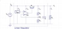
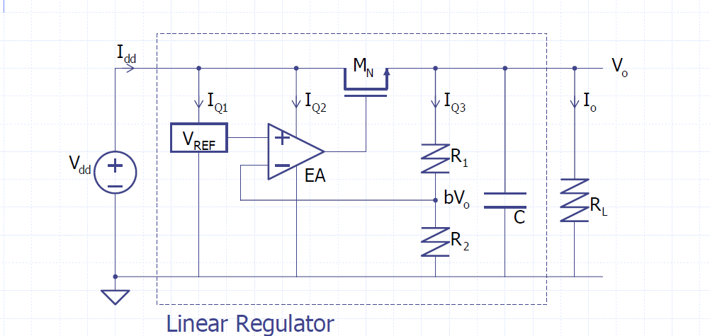
I have been trying to understand a series of equations I have come across. The equations deal with dropout voltage of a linear regulator with a NMOS pass device. Below is the schematic of the generic linear regulator.


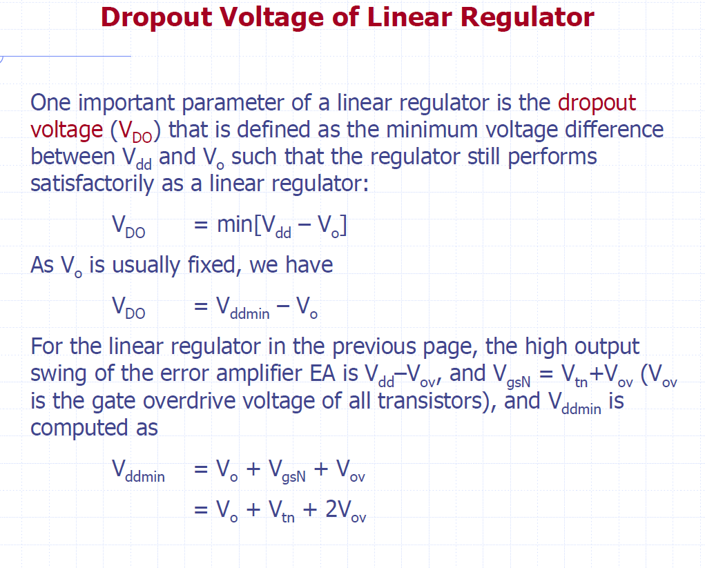
The second picture below has the slide which has the equations.


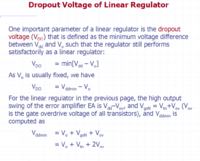
I get the first two equations that dropout voltage is equal to Vdd min (input voltage min) minus the output voltage Vo.
What I don't get is how for the third equation for Vdd min has the gate-source voltage of the NMOS pass device, VgsN. Shouldn't Vddmin just be Vov + Vo? Why care about the gate to source voltage drop?
 
Last edited by a moderator:

If you copy and paste the links, they work.

................What I don't get is how for the third equation for Vdd min has the gate-source voltage of the NMOS pass device, VgsN. Shouldn't Vddmin just be Vov + Vo? Why care about the gate to source voltage drop?
Because in that circuit the NMOS is acting as a source-follower, so the voltage drop across it cannot be less than Vgs required to turn on the transistor.
 

Thanks for taking the time to edit my post and redo the pictures BradtheRad. Appreciate it.


If you copy and paste the links, they work.

Because in that circuit the NMOS is acting as a source-follower, so the voltage drop across it cannot be less than Vgs required to turn on the transistor.

thanks for taking the time to reply.

so correct my if I am wrong. Since the pass device is NMOS a certain Vgs should be applied to it to turn it on (which is drawn from Vddmin).
So when calculating the dropout voltage Vdo = Vddmin - Vo = Vgs + Vov.

Is this right?

For a PMOS pass device there is no Vgs or Vsg term because a low voltage value or zero turns it on. Am I right here ?
 

The P-device works in symmetry to an N-device.
Bias is referenced to the more positive leg.
We get voltage regulation from a P-device by putting the load in the leg close to the positive rail.
It provides current regulation with the load in the leg near the negative rail. As you state, the load can go down to 0V.
 

A pmos has roughly the same Vgs as an nmos, the difference is where the S is. In the nmos situation the S is the output which means the gate must be one Vgs threshold above that. That sets up a minimum dropout.

If the pass transistor was pmos it would need a similar Vgs (though negative) but the S would be Vdd. In this situation the dropout voltage would have nothing to do with Vgs and dropout could ideally approach zero (limited by the on-resistance of the PMOS). Instead a new constraint would arise where Vdd would have to be greater than the pmos Vgs threshold.
 
  • Like
Reactions: tenso

    tenso

    Points: 2
    Helpful Answer Positive Rating
A pmos has roughly the same Vgs as an nmos, the difference is where the S is. In the nmos situation the S is the output which means the gate must be one Vgs threshold above that. That sets up a minimum dropout.

If the pass transistor was pmos it would need a similar Vgs (though negative) but the S would be Vdd. In this situation the dropout voltage would have nothing to do with Vgs and dropout could ideally approach zero (limited by the on-resistance of the PMOS). Instead a new constraint would arise where Vdd would have to be greater than the pmos Vgs threshold.

thanks for the post and explanation. it helps a lot. If I understand the last line correctly then you are saying that the source voltage for PMOS pass transistor should be greater than the gate voltage such that Vsg > vth at least.
 

Yes, that's how a PMOS works and how it differs from an NMOS. PMOS turn on with a negative Vgs.
 

NMOS needs VTN plus sqrt(Id)/k' (plus a skosh for
Ron*Id, if it's that far buried) above the Vout. This
is why you see many "ULDO" designs with a low
voltage output supply and a higher voltage VAUX
supply to run the pass FET gate drive.

PMOS LDOs drive the gate toward ground and at
very low VIN, fail to drive the gate adequately.
That's where you switch over to the ULDO (NMOS)
style.
 
  • Like
Reactions: d123

    d123

    Points: 2
    Helpful Answer Positive Rating
NMOS needs VTN plus sqrt(Id)/k' (plus a skosh for
Ron*Id, if it's that far buried) above the Vout. This
is why you see many "ULDO" designs with a low
voltage output supply and a higher voltage VAUX
supply to run the pass FET gate drive.

PMOS LDOs drive the gate toward ground and at
very low VIN, fail to drive the gate adequately.
That's where you switch over to the ULDO (NMOS)
style.

Thanks for the feedback. Just some additional questions.

1) what is skosh?
2) Is it common for the VAUX to be higher than the input voltage at the drain? I think in some designs you boost the gate voltage of the pass device using charge pumps.
 

Status
Not open for further replies.

Part and Inventory Search

Welcome to EDABoard.com

Sponsor

Back
Top