Continue to Site

Welcome to EDAboard.com

Welcome to our site! EDAboard.com is an international Electronics Discussion Forum focused on EDA software, circuits, schematics, books, theory, papers, asic, pld, 8051, DSP, Network, RF, Analog Design, PCB, Service Manuals... and a whole lot more! To participate you need to register. Registration is free. Click here to register now.

High Side Driving Boost Voltage Ciruit

Status
Not open for further replies.

MangoKid

Junior Member level 1
Joined
Dec 8, 2010
Messages
17
Helped
3
Reputation
6
Reaction score
3
Trophy points
1,283
Activity points
1,393
I am trying to create a circuit to generate the boost voltage for mosfet highside driving. Instead of using gate drivers or individual boost circuits for for each highside mosfet I want to create one centralized boost power supply. This is because there are 30 half bridges on the board.

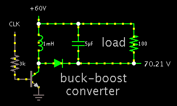
I was thinking of using an LM5022 to create the boost voltage. However I want the boost voltage to be about +10 above VP. The LM5022 will output a fixed voltage which is no good for this application because the VP voltage will change over a large range. I think there must be a way of configuring the LM5022 to be some voltage above the input voltage. Its a bit beyond my knowledge so I thought I would seek some help.

Thanks!
 

My first thought of a flyback with bais coil control and 30 (or more) secodaries is going to be a little unrealistic, so therefore i think you need loads of bootstrap high side drivers or pulse transformer high side drives, for each half bridge.
What is power of each half bridge?, what is switching frequency? What is Vin and Vout to each half bridge?
 
Vin will be max 60
Vout will be max 60
Switching frequency is 20Khz Max
Each bridge will handle up to 20A

I haven't selected the mosfets yet.

Each half bridge will be at the same voltage, the wont each be at a different voltage. I think I can generate what is needed with the LM5022 but I need to figure out how to control the internal comparator so the voltage is vin+10v.

- - - Updated - - -

I think a flyback converter will work. I don't need multiple taps because there is only one vin.

Now I just have to figure out the capacity of the flyback.
 

Hi,

In my eyes: High side drive voltage needs to be independent for each halfbridge, because the voltage must move with halfbridge output voltage up and down.

But maybe you have a solution for a common supply. I wonder how it looks like.

Klaus
 

Bootstrapping with a proper driver solves the problem of high side gate drive supply with minimal components. There are a few cases you can't use it, but I don't see anything to indicate this is one of them.
 
  • Like
Reactions: treez

    T

    Points: 2
    Helpful Answer Positive Rating
I want the boost voltage to be about +10 above VP

A buck-boost converter can be arranged so it is referenced to the positive rail. Its output is that much greater than the supply rail. So if the supply is 60V, and you regulate the buck-boost load to 10v, it is at 70V relative to ground.

My schematic is only a guess about how your load draws current. A light load can be referenced to 0V ground.

5782656500_1485312756.png
 
  • Like
Reactions: treez

    T

    Points: 2
    Helpful Answer Positive Rating
Bootstrapping with a proper driver solves the problem of high side gate drive supply with minimal components. There are a few cases you can't use it, but I don't see anything to indicate this is one of them.

Yes, the "approach" of the original post is however to use a single, non-isolated power supply for multiple high side drivers.
Instead of using gate drivers or individual boost circuits for each highside mosfet I want to create one centralized boost power supply.

I agree with KlausST, this can't work.
 
  • Like
Reactions: treez

    T

    Points: 2
    Helpful Answer Positive Rating
For driving 30 half bridge high side mosfet, best idea is to create different ground and isolate the input pulse from circuit using opto-coupler or pulse transformer.


Hi,

please reconsider the idea of generating a common high side drive voltage supply.

How do consider to limit V_GS of each single MOSFET?
How do you consider to limit current and power dissipation (SOA) of the gate driver individually?
Avoid that a fail on one halfbride influences other halfbridges.

Klaus
 

Status
Not open for further replies.

Part and Inventory Search

Welcome to EDABoard.com

Sponsor

Back
Top