Continue to Site

Welcome to EDAboard.com

Welcome to our site! EDAboard.com is an international Electronics Discussion Forum focused on EDA software, circuits, schematics, books, theory, papers, asic, pld, 8051, DSP, Network, RF, Analog Design, PCB, Service Manuals... and a whole lot more! To participate you need to register. Registration is free. Click here to register now.

Why has our Flyback SMPS transformer got so many strangely connected shield windings?

Status
Not open for further replies.
T

treez

Guest
Hello,
Please could you advise why there are two strangely connected shield windings in our Offline Flyback transformer?
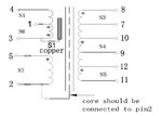
There are two shield windings in the transformer as shown in the transformer diagram attached to this post.
This Flyback SMPS is 67W and VAC input is 100VAC to 265VAC.
The output charges up to 340V, so to make the voltage reflected to the primary less, the designer used three separate secondaries (N3, N4 and N5) and “stacked” their outputs. (as shown in the schematic attached).
It actually appears that the two shield windings are connected in a manner which we would not want. I thought that shield windings were just supposed to connect to a single place, eg primary or secondary ground or power?
What is the purpose of doing the shield windings as in the attached transformer diagram?

(LTspice simulation also attached though not needed)
 

Attachments

  • Transformer diagram.jpg
    Transformer diagram.jpg
    41.2 KB · Views: 266
  • Flyback SMPS.pdf
    22.4 KB · Views: 137
  • Flyback SMPS.TXT
    10.1 KB · Views: 95
Last edited by a moderator:

Hi,

Often this is done to
* increase safety
* reduce primary switching noise coupling to secondary side.

Safety: if a primary winding burns ... then one has to avoid a connection to the secondary side.
The extra winding makes a fuse to blow before the dangerous voltage reaches the secondary side.

Noise: the primary side is switching with high voltage high dU/dt. There is a capacitive coupling between primary and secondary winding...this causes common mode noise at the secondary side with respect to earth ground. The winding can't decrease the capacitance, but the coupling now is against earth ground, which is considerd noise free.

Klaus
 
  • Like
Reactions: treez

    T

    Points: 2
    Helpful Answer Positive Rating
The transformer diagram is useless without an application circuit. The shield connect to pin 3 makes sense if pin 3 is connected to primary Vdc+. What's N2?.

Your circuit has no isolation, thus it doesn't need shields at all.
 
  • Like
Reactions: treez

    T

    Points: 2
    Helpful Answer Positive Rating
Your circuit has no isolation, thus it doesn't need shields at all.
Thanks, the real circuit does have isolation, sorry about that.

What's N2?.
N2 is the auxiliary coil, grounded to pri ground.
The shield connect to pin 3 makes sense if pin 3 is connected to primary Vdc+.
Thanks, they have connected pin 3 to the drain of the power FET not to primary power.
 
Last edited by a moderator:

I am just curious, the winding between pin 1 and 3 has got dot on both ends (that is marked N6). - how do you wind such a coil?
 

The windings polarity suggests that N3 is the "switching" drain node. If so, S1 is in fact wrongly connected to act as a shield. It's also not clear what exactly connects to pins 2. The ferrite core can at best be used to steer electrostatic low frequency fields but is no effective shield for switching frequency.

To reduce injected switching frequent currents between primary and secondary, we would in fact want a double screen, connect each to primary and secondary ground.

I am just curious, the winding between pin 1 and 3 has got dot on both ends (that is marked N6). - how do you wind such a coil?
Consider a misplaced dot. O.k., doesn't make the drawing look very trustworthy.
 

Consider a misplaced dot. O.k., doesn't make the drawing look very trustworthy.

One more puzzle: in a ferrite core transformer, how do you connect to the core? And the core itself is non-conducting. You cannot solder or weld to the ferrite core!

The screen should be connected to the ground, if you want it to work as expected.
 

The boss says that the shied winding should be connected to the switching node of the flyback SMPS. He says that where you connect the shield winding to depends on what kind of shielding you want.
 

The boss says that the shied winding should be connected to the switching node of the flyback SMPS.
Is it so? I don't see a reasonable purpose of this kind of "shielding".
 

... He says that where you connect the shield winding to depends on what kind of shielding you want.

The boss knows best but a real engineer has really few options...
 
  • Like
Reactions: treez

    T

    Points: 2
    Helpful Answer Positive Rating
All we can do is guess about the shield connections without more data. I would think the shield on the core is really a belly band. Do you have a transformer to look at? You should also add the transformer pin numbers to your schematic.
 
  • Like
Reactions: treez

    T

    Points: 2
    Helpful Answer Positive Rating
...I would think the shield on the core is really a belly band. ...

I agree - it just acts like a Faraday cage and there is no need to connect it to anywhere. It stops only the electric field but allows the magnetic field to pass. You need to ensure that you do not make short circuit for the eddy currents.
 
Last edited:
  • Like
Reactions: treez

    T

    Points: 2
    Helpful Answer Positive Rating
A shield can serve safety or EMI purposes, but I've never seen a configuration where any shield is connected to the switching node. It will likely only increase common mode interference.

Grounding the "belly band" on the core might have a positive effect on common mode interference, especially if split windings are used.
 
  • Like
Reactions: treez

    T

    Points: 2
    Helpful Answer Positive Rating
Status
Not open for further replies.

Similar threads

Part and Inventory Search

Welcome to EDABoard.com

Sponsor

Back
Top