asdf44
Advanced Member level 4
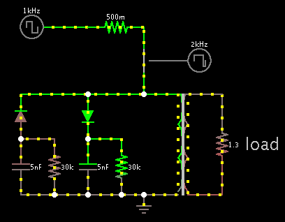
I want to discuss snubber design/topology for a phase shifted full bridge adapted for an inverter (DC-1khz) application with about 30A output at ~750w. This is the basic topology with my current simple RC snubber shown:

One key detail is that the back to back switches effectively remove the body diodes from the picture so there is no natural clamping on the secondary. Second, the fact that the output can be AC eliminates some common snubbers for the full bridge topology (Like diode->cap that drains to the output).
The design right now is roughly as follows
400V primary -> 26:2 transformer -> 30V secondary -> 60V secondary blocking voltage + voltage ringing -> ~130V -> 150V mosfets.
This, overall, is workable according to simulation with about 10W of snubber losses but obviously doesn't have much margin. So cutting down on secondary voltage overshoot would have significant benefits in terms of design margin, and/or allow another turn in the secondary for additional voltage capability or allow lower voltage fets with the obvious benefits that brings.
So does anyone have general comments or suggestions for snubber design/topology in this application (or other comments on the desire to limit voltage at the secondary fets). PSFB has plenty of literature but not with a bipolar secondary. I can invent things, but I'd rather not. Note that the schematic as drawn also roughly represents planned layout.