electroman2000
Member level 2
Hi everyone, I applied for a job as layout engineer. The job spec are the following:
DUTY:
-schematic to full custom layout translation
-layout verification and DRC
-floor planning for optimal die area
-generation of wire bonding diagram for assembly approval before the tape-out
REQUIREMENTS:
-EE degree with focus on microelectronics
-good knowledge of CMOS/BiCMOS and schematic-layout translation
-cadence virtuoso
Then there is other spec for senior, but I'm applying as junior.
I haven't experience with analog integrated circuite design, but I studied a lot digital integrated circuit, and also subject like solid state physics and semiconductor devices, so I know problems that can arise.
They decide to interview me anyway. First question was about CMOS cross section, all ok. Second question about Latchup, all ok. Third question about mismatching...I didn't know what mismatching was, then I answer (based on my digital design knowledge) that MOS (wheter NMOS or PMOS) have to be placed at the same distance and with a simmetry, to avoid different RC value of the connection wires. After the interview I read about mismatching, and even if what I said is not incorrect, is not related with mismatching.
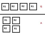
For the last question, look at this image: up is the question, down is the answer:

I didn't understand the question very well, because for first he drow a PUN with 4 transistor in parallel, and then a PDN with a resistor, then during the explanation he drow a voltage divider and said that each resistor is composed by 2 resistor, and then he drow that 4 resistor as in figure, saying that both R1 is affected by variation (e.g. in the dopant level), and asked me to rearrange the layout in order to minimize the impact. I never ever do that, so I try to do it like a puzzle, finding the best simmetry for the system, so I drow like the layout below. He said "OK, for me is enough" and so at the beginning I think it was correct...but later, I still have no idea why, physically, it avoids the problems...however I found the same structure in a slide called "common centroid arrays" so I think my intuition about the symmetry was correct.
Could you tell me if my last two answer was correct?
However, they tell me in a week the response, and if it was good I have to go there for a 1:1 interview. So it will pass for sure 2 weeks. Could you please suggest me what to study and from where the analog design, based on the spec that I wrote above?
Thank you very much
DUTY:
-schematic to full custom layout translation
-layout verification and DRC
-floor planning for optimal die area
-generation of wire bonding diagram for assembly approval before the tape-out
REQUIREMENTS:
-EE degree with focus on microelectronics
-good knowledge of CMOS/BiCMOS and schematic-layout translation
-cadence virtuoso
Then there is other spec for senior, but I'm applying as junior.
I haven't experience with analog integrated circuite design, but I studied a lot digital integrated circuit, and also subject like solid state physics and semiconductor devices, so I know problems that can arise.
They decide to interview me anyway. First question was about CMOS cross section, all ok. Second question about Latchup, all ok. Third question about mismatching...I didn't know what mismatching was, then I answer (based on my digital design knowledge) that MOS (wheter NMOS or PMOS) have to be placed at the same distance and with a simmetry, to avoid different RC value of the connection wires. After the interview I read about mismatching, and even if what I said is not incorrect, is not related with mismatching.
For the last question, look at this image: up is the question, down is the answer:

I didn't understand the question very well, because for first he drow a PUN with 4 transistor in parallel, and then a PDN with a resistor, then during the explanation he drow a voltage divider and said that each resistor is composed by 2 resistor, and then he drow that 4 resistor as in figure, saying that both R1 is affected by variation (e.g. in the dopant level), and asked me to rearrange the layout in order to minimize the impact. I never ever do that, so I try to do it like a puzzle, finding the best simmetry for the system, so I drow like the layout below. He said "OK, for me is enough" and so at the beginning I think it was correct...but later, I still have no idea why, physically, it avoids the problems...however I found the same structure in a slide called "common centroid arrays" so I think my intuition about the symmetry was correct.
Could you tell me if my last two answer was correct?
However, they tell me in a week the response, and if it was good I have to go there for a 1:1 interview. So it will pass for sure 2 weeks. Could you please suggest me what to study and from where the analog design, based on the spec that I wrote above?
Thank you very much