Continue to Site

Welcome to EDAboard.com

Welcome to our site! EDAboard.com is an international Electronics Discussion Forum focused on EDA software, circuits, schematics, books, theory, papers, asic, pld, 8051, DSP, Network, RF, Analog Design, PCB, Service Manuals... and a whole lot more! To participate you need to register. Registration is free. Click here to register now.

[SOLVED] Very Low Differential voltage amplification

Status
Not open for further replies.

Fabien

Full Member level 1
Joined
May 22, 2011
Messages
96
Helped
10
Reputation
20
Reaction score
10
Trophy points
1,288
Location
Grenoble
Activity points
2,025
Dear all!

I'm trying to amplify a differential signal what may vary from a few hundreds of micro-volts to tens of milli-volts. The main challenge is to design this amp in sub 1V and in sub 1µA.
I designed OpAmp but won't work with such a low input voltage.
The only way I found is to amplify separately these two differential signals (ie. with a cascode amp) and then amplify it with OpAmp (but it requires two casc amp and 1 opamp).
An other amplifier I tried is a double diff amp (one differential pair whose outputs is connected to an other differential pair). It almost work but there is a long delay (once the differential signal is below zero, the output of this double diff amp wait half a micro-sec to decrease).

Question : What kind of amplifier (it also could be a comparator) could I design for such a low input voltage? (I tried with INA but... gave-up).
 

Hi, I would use an INA since they are used for small signal purposes, try INA141, adjusting the gain is simply a means of using a variable resistor.
 

Hi, I would use an INA since they are used for small signal purposes, try INA141, adjusting the gain is simply a means of using a variable resistor.


Thank you for reply, but by design I mean Analog Integrated Circuit Design. So, if you know the design of the INA141, it could be interesting ;)
 

Thank you for your answer.
I'll read it and try to simulate this kind of design. Hopefully it will be suitable for my needs.
 

Hi,

I have no experience with IC design.

But often low power means a lot of noise.

You should specify your input signal:
What common mode voltage range?
What differential voltage range?
What supply voltage?
What input signal frequency range?
Are you interested in DC precision or AC only?
What input source impedance?
What voltage noise and current noise is acceptable?

I did a lot of signal amplification applications:
For low frequency maybe a chopper stabilized circuit is good.
For low impedance AC source and low noise a bjt input stage (high current) is good.
For high impedance source input a FET input stage is good.

Klaus
 

Yeah, you are right! As lowest is the power, as highest is the noise! These are the main trade-off in my design!

For my input signal:
The common mode voltage, I setted it around 0.5V (Vdd/2). The differential voltage is around 0.8V for the positive and 0.3 for the negative. I DC bocked and added Vbias for 0.5V
The supply voltage (Vdd) is 1V (or slightly below).
The frequency range is quite low, from 100kHz to 1MHz.
No care of DC precision. Just need to amplify (without adding lot of noise ;) ) the signal.
Input source impedance should be high (MOS grid for example) in order to avoid the input signal decrease.
No real idea for the moment about the voltage or current noise.

"I did a lot of signal amplification applications:
For low frequency maybe a chopper stabilized circuit is good. GOOD idea, I thought abt it, but need a clock (not excluded cause I just designed one for an other part of the project).
For low impedance AC source and low noise a bjt input stage (high current) is good. Impossible, no bjt in my design kit!
For high impedance source input a FET input stage is good. Like MOS, input differential pair for example, but the one I did won't amplify below 1mV."

Klaus[/QUOTE]
 

No real idea for the moment about the voltage or current noise.
Perhaps you should review the transistor data of your design kit. You can calculate expectable voltage and current noise for specific transistor size and drain current.
 

Perhaps you should review the transistor data of your design kit. You can calculate expectable voltage and current noise for specific transistor size and drain current.

Humm... You'r probably right! I calculated the noise only for the input device (before the amplifier) maybe I should try to compute/simulate the noise generated by the amp (the input pair) in order to know the level of noise regarding to the signal. I'll do that tomorrow and will give more updates.
 

which technology are you using ? tsmc , umc ? cmos or bipolar ? 0.18u ? 0.13u ?

I tried to simulate ones again my netlist but not able to know remove the noise generated by the input pair.
Techno CMOS 28nm - FDSOI
 

I did a simple 2 stage opamp design:

op1.png

op2.png

DC gain: 78dB

UGB :1.8 MHz

PM: 57 deg

Total current : 900 nA

VDD = 1v

it is designed in 180nm you can design in 28nm :)
 

I did a simple 2 stage opamp design:

View attachment 132632

View attachment 132633

DC gain: 78dB

UGB :1.8 MHz

PM: 57 deg

Total current : 900 nA

VDD = 1v

it is designed in 180nm you can design in 28nm :)

Thank you for this design, that's interesting! Most of your MOS are working in subthreshold.
Actually, I did this kind of design, with input pair un sub-th (gm/Id in 28nm reaches 35!) and I got more than 100dB at DC gain! I think it could be a common mode trouble, I'll try to get some more informations about this...
 

It depends on ur design u can get better gain but lower bandwidth. U can increase ur lengths and evade subt region.

And btw all transistors are working in sat not subt. U can check in cadence the region for all is 3 which is sat. :)

If u have hspice models of ur transistors give them to me i can do in ADS.

check this:

op3.png
 
Last edited:

You'r right, they are in sat... but you can be both, in sub-th an still be in sat (Vgs < Vth but Vds > Vdsat).
I'm not trusting anymore the cadence Operating mode since it gives me wrong info.

Here is my differential input signal. I dc block and add biasing (Vdd/2).


Vin_Diff.png
 

You'r right, they are in sat... but you can be both, in sub-th an still be in sat (Vgs < Vth but Vds > Vdsat).
I'm not trusting anymore the cadence Operating mode since it gives me wrong info.

Here is my differential input signal. I dc block and add biasing (Vdd/2).


View attachment 132642

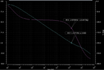
ur right but i have higher vths in ur tech probably vths are low. Also u can decrease w/l ratios. it is easy.

I do not understand ur waves they do not have labels ... :)

- - - Updated - - -

here u go now all are in sat.

op1.png

op3.png
 

Sorry, I missed the labels (The first is the positive signal, second negative). I remove the DC and add bias at 500mV (the next 2 signals). The last one, well, it's the output that should be rail to rail.
Thank you for your design below 800nA! I can see your miller cap for stabilisation, I reallized my amp wasn't stabilized at all! I'll try to retune my OpAmp.
So you think your OpAmp can amplify such a low input differential signal?
 

bad news ! ur gain will be less than 25 db !

u want to have good gain in 1Mhz and have total current like 1u !!!!!!!!!!!

I am worried that is not possible !!!!


for example u need a 40dB gain in 1Mhz. Imagine that ur corner frequecny is 1Mhz.

40db means 100 gain then ur unity gain bandwidth should be 100Mhz !!!!!! u cant reach this bandwidth with 1uA current !
 

Status
Not open for further replies.

Part and Inventory Search

Welcome to EDABoard.com

Sponsor

Back
Top