Continue to Site

Welcome to EDAboard.com

Welcome to our site! EDAboard.com is an international Electronics Discussion Forum focused on EDA software, circuits, schematics, books, theory, papers, asic, pld, 8051, DSP, Network, RF, Analog Design, PCB, Service Manuals... and a whole lot more! To participate you need to register. Registration is free. Click here to register now.

Stb and AC analysis don't match

Status
Not open for further replies.

afonsom

Newbie level 5
Joined
Aug 16, 2016
Messages
10
Helped
0
Reputation
0
Reaction score
0
Trophy points
1
Activity points
86
Hi everyone,

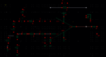
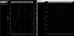
This is the first time I'm designing a differential amplifier on Cadence (an amplifier for a neural probe) and after doing a stability analysis something strange happened: The loop gain doesn't correspond to the gain I obtained when doing an AC analysis (the one I desired) and I truly don't understand why. I leave the print of the simulations and the circuit schematic attached.
Thanks for everything!

EDIT: Another question, if you look at my AC plot, my midband gain (from 1k to 50k approximately) is not flat at all. I think this behavior happens because of the neural electrode model (represented by the capacitor in series with the resistor in the schematic) and I don't know any method to flatten the response.
 

Attachments

  • schematic.PNG
    schematic.PNG
    23.6 KB · Views: 510
  • simulation.PNG
    simulation.PNG
    63 KB · Views: 594
Last edited:

Hi,

Why are you AC coupling the inputs? I believe that this your problem, since you have only positive supply you need to have some DC offsets on the inputs.
 

I have run into similar problems with stb, like it starts at
a solution of no gain rather than peak gain. Never did get
to understand why; expedience pushed me back to the
old familiar AC method and calculator extraction of the
gain & phase. It wasn't a consistent failure either, just
enough of them in PA/MC loops to make the results look
unreliable.
 

At first, it is correct and necessary to use capactive input coupling. Only in this case. the DC non-inverting gain is unity (good for single supply operation).
Secondly - how did you simulate the loop gain? It must start at Aol (open-loop gain of the opamp) due to unity gain dc feedback.
Remember: Loop gain is the gain around the feedback loop which - for measurement or simulation purposes - has to be opened at a suitable point.
 
Last edited:

Hi,

Why are you AC coupling the inputs? I believe that this your problem, since you have only positive supply you need to have some DC offsets on the inputs.

C9 and C10 capacitors are needed to represent the model of the neural electrode. C19,C20,C21,C22 are used to implement an high pass filter because I wish to cut out DC. I have some DC offset on the input inside the opamp itself. Thanks!
 
Last edited:

At first, it is correct and necessary to use capactive input coupling. Only in this case. the DC non-inverting gain is unity (good for single supply operation).
Secondly - how did you simulate the loop gain? It must start at Aol (open-loop gain of the opamp) due to unity gain dc feedback.
Remember: Loop gain is the gain around the feedback loop which - for measurement or simulation purposes - has to be opened at a suitable point.

Hi. C9 and C10 actually represent the neural electrode model while the other capacitors are used to implement an high pass filter.
To simulate the loop gain I just placed the probe in a location that opens up the loop. This was the first time I've simulated the loop gain, am I missing something?
Also, do you know how could I have a flattened midband gain? It seems to be impossible to avoid this behavior because of the electrode model.
Thanks for everything!
 

In AC analysis , iprobe is ignored(shorted). Hence probing ac response on the output node will give you closed loop response and not the open loop response.

In Stb analysis, first dc operating point is evaluated (i.e. any ac signal is set to 0V), then small signal transfer response from "iprobe's" one terminal(+ve node) to the other terminal (-ve node) is reported. This basically is open loop response of the loop containing the "iprobe".

Hi! Everything you said makes sense and I undestand how it works now. But do you have any idea why the loop gain (A*Beta) that I've obtained is negative (in dB)? This mean the loop gain has crossed 0dbs close to DC so the system is unstable?
Thanks for everything!
 

Hi! Everything you said makes sense and I undestand how it works now. But do you have any idea why the loop gain (A*Beta) that I've obtained is negative (in dB)? This mean the loop gain has crossed 0dbs close to DC so the system is unstable?
Thanks for everything!

According to your own words - something with the loop gain response seems to be wrong.
Question: Why you don`t clearly show or describe how do you have simulated the loop gain (instead of speaking only about a "probe" and a "location").
The loop gain must start (at low frequencies) with a very large value and the phase shift must be -180deg.

In order to simulate the loop gain I simply placed the iprobe in a location that opens up the loop (as shown in the schematic) and did a stability analysis from 0.1Hz to 1GHz. After that, I plotted the loop gain (magnitude and phase). I'm really inexperienced when it comes to designing amplifiers and it shows, maybe I'm missing some steps that I didn't take into account and that's why the Loop Gain doesn't look the way it should. Thanks for everything.
 

In order to simulate the loop gain I simply placed the iprobe in a location that opens up the loop (as shown in the schematic)

For simulating the loop gain of a system involving voltage transfer functions you must not use a current probe but a voltage probe, of course.
 

For simulating the loop gain of a system involving voltage transfer functions you must not use a current probe but a voltage probe, of course.

The problem is that there isn't a voltage probe in analoglib, only the iprobe, that's why I assumed it was the only option.
Very grateful for your help by the way.
 

You need simply an ac voltage source - not available in analoglib?
 

You need simply an ac voltage source - not available in analoglib?

I'm sorry because it seems I'm completely missing the point. Are you talking about replacing the iprobe with an ac voltage source and using that as the probe for my stb simulation? I've done so and set the AC magnitude of this ac voltage source to 1V. However, it seems the loop gain (magnitude and phase) are still off specially because it seems the compensation of the op-amp doesn't seem to have any effect on the stability. I've attached the test-bench and the loop-gain plot. Again, I can't thank you enough for your help.

https://obrazki.elektroda.pl/4978691700_1472574522.png
https://obrazki.elektroda.pl/9944806800_1472574523.png
 

For loop gain simulation, perform the following steps:
* Set all input signal sources to zero;
* Place an ac voltage source (1V) between opamp output and feedback path;
* Display vs. frequency the RATIO V(signal,out)-to-signal,in. In your case: V(out)/V(8).

Did you follow this procedure (including step 1)?

Yes, I followed this procedure, and the V(out)/V(8) vs. frequency print was the following:

https://obrazki.elektroda.pl/5436736700_1472583090.png

For me, it still doesn't make any sense or my interpretation of the graph is flawed. Taking into account the AC response of V(out)/V(7) and the tran response I was expecting a perfectly stable circuit which is not what this plot entails.
 

Only now I have recognized that you are working with single supply.
But I cannot verify a correct input biasing with Vdd/2.
Did you check the DC operating point?
 

Only now I have recognized that you are working with single supply.
But I cannot verify a correct input biasing with Vdd/2.
Did you check the DC operating point?

Yes, I've checked the DC operating point and every mosfet is in saturation. I biased the input transistors using large drain-to-gate feedback resistors, in this case implemented using pseudo pmos resistors. This is the schematic of the op-amp. but I don't think the problem is here. It's a simple two-stage amp.

https://obrazki.elektroda.pl/2014588400_1472593065.png
 
Last edited:

What is the DC value of the output voltage with feedback?
 

Status
Not open for further replies.

Similar threads

Part and Inventory Search

Welcome to EDABoard.com

Sponsor

Back
Top