Continue to Site

Welcome to EDAboard.com

Welcome to our site! EDAboard.com is an international Electronics Discussion Forum focused on EDA software, circuits, schematics, books, theory, papers, asic, pld, 8051, DSP, Network, RF, Analog Design, PCB, Service Manuals... and a whole lot more! To participate you need to register. Registration is free. Click here to register now.

Proper GND distribution with power electronics

Status
Not open for further replies.

bremenpl

Member level 3
Joined
Jan 5, 2013
Messages
63
Helped
0
Reputation
0
Reaction score
0
Trophy points
1,286
Activity points
1,827
Hello there,
I am trying to find some resources regarding PCB design layout for projects including power electronics components, for example high current mosfets for motor driving etc. In general I have the following questions:

  1. When creating a 4 layer PCB (middle layers are plane layers), should one pour GND over outer signal layers? Apart that I think it simply gives more conductivity and lowers the GND path resistance, can it do any harm?
  2. In a circuit when both digital and analog circuits are on board, it is recommended to separate analog GND with digital GND plane and only connect them in one place (star design). Does this apply also to power electronics GND? Should the GND be separated as well?

I would appreciate all help.
 

Separating GND kinds (power, analog, digital) is always welcome for signal integrity purpose, but how strict and how efficient necessary, it depend on design requirements, component specifications and dynamic aspects such as energy level involved and bandwidth of signals.
 

The frequencies on the board are up to 30kHz (transiators switching). Maximum expected currents are 5-6A.
 

Hi,

should one pour GND over outer signal layers?
I often see this. But I´m no froend of it. I recommend a solid GND plane in an inner layer (or bottom layer if there are no comonents).

Place your components in away that there are dedicated "power areas", "digital areas" and "analog areas".
A good start is if all three are connected at a star point close to the power input near the power supply bulk capacitors.

You can route your PCB and upload a picture, so we can comment it.


Klaus
 

The rules are like this…and do whatever you have to do to abide by the.
Keep all high di/dt power switching currents well confined….
Keep the loops of current where high di/dt switching current flows as small in area as possible.
Don’t let high di/dt power switching currents run through lengths of control ground as you will get ground bounce.
Keep all current loops as narrow in area as possible (have go and returns closely together)
If you have a chip somewhere, then it will have a ground….and any of the circuitry that inputs to that chip should best have the “same” ground as that chip, and not have their ground bouncing around in relation to the chip’s bit of ground.
 

Hi,

I hope, along with the above great advice and recommendations, some of these may help.

I only know about keep return paths as short as possible, is one, that's good to learn about for layout; and then the above of separating the board into sections (imaginary quadrants, let's say), not mixing analog and power or digital if poss, I think I remember power guzzlers should go as close to the pcb supply input as possible, and a single ground plane, separate regulators can be helpful if possible and not too OTT in number.
 

Attachments

  • PCB layout and design.rar
    5.7 MB · Views: 92

Thank you for the answers. So for example, I have a H bridge mosfet circuit. I measure current there using sense resistor and instrumentation op amp. Also there is a high side circuit attached to drive the top N fets. Those circuits are close to eachother obviously. Should I care to ibject separate ground to each: mosfet, op amp and high side bridge circuit? Or should I threat it all as "power" circuit and just separate its ground from mcu circuitry?
 

Hi,

I assume there is no general answer...

Often it's good to amplify the current signal referenced to the power GND, then feed the signal to the analog section.
Otherwise you additionally amplify the difference between both GNDs ... obviously amplifying the "error"..

Klaus
 

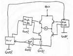
I will try to make the question less generic. I have attached a small sketch of a system I am working on. I have added question marks at the end of each GND terminals. Which GND terminals should be the same?
For example in my current PCB design, all components are very close to each other, making it really only possible to separate the MCU GND port. The other 4 GND's would have to be the same "potential".
Looking forward to your notes about it.

GNDs.png
 

Hi,

Screenshot_2016-08-06-11-33-18.jpg

My idea:
* first check your current measurement path of full bridge
* P means power GND
* C means microcontroller GND
* then I used a difference amplifier circuit, this theoretically cancels all grond bounce.

Klaus

Added:
Connect driver circuits to power GND
 

Thank you for answer. So if I understand correctly the gnd of op amp doesnt matter since its a differential op amp anyway? Only ref voltage matters (gndc in your example)?
 

Hi,

I'd refer the Opamp supply to the cleaner GND --> microcontroller GND.

Klaus
 

Ill try to manage that. Thank you a lot.
 

Status
Not open for further replies.

Similar threads

Part and Inventory Search

Welcome to EDABoard.com

Sponsor

Back
Top