Continue to Site

Welcome to EDAboard.com

Welcome to our site! EDAboard.com is an international Electronics Discussion Forum focused on EDA software, circuits, schematics, books, theory, papers, asic, pld, 8051, DSP, Network, RF, Analog Design, PCB, Service Manuals... and a whole lot more! To participate you need to register. Registration is free. Click here to register now.

Help plz: Class AB OTA design in 28nm

Status
Not open for further replies.

watch_back

Newbie level 4
Joined
Jun 13, 2016
Messages
7
Helped
0
Reputation
0
Reaction score
0
Trophy points
1
Activity points
64
Hi
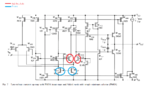
I have a specification as high gain (80db), fast settling few ns, good PM.
I have gone through several topolgoies. One of them I am considering now is from Huijsing's book having a folded mesh with a minimum selector.
Unbenannt.PNG

If I use Regular PMOS NMOS devices I can't manage to keep all of the transistor in saturation as there is less voltage headroom.
Instead I used high performance low threshold devices. Still I am not reaching the specification.

So far I have 60db gain with 550mv of output swing, 500uw DC power with high performance device. I can't increase the gain because then I have to compromise with my output voltage swing.

by using regular devices I am only getting 40db gain. Could you please help me about this? I am missing something really important as I am a beginner with the analog design. Any simplest feedback will be appreciated :)
 

First of all You have to understand how current mirrors works. Then, understood at least one high swing cascode CS and use them as load of your opamp.
For this configuration 60dBs of open loop gain with shortest regular devices should be achievable (with 1GHz of GBW for this power and not too high load - sthing like a 1pF)
 
Hi Dominik,
Thank you for the comment. I have studied current mirrors. So far I am playing with the W/L of transistors. One good point you said is the high swing of cascode. Could you give me some hints about it or any tutorial might be helpful as well.

For this configuration 60dBs of open loop gain with shortest regular devices
..............did u mean that instead of 40db (what I am getting now can be improved further) can be enhanced to 60db?

If it is so...still I need to raise 20db. how do u suggest that to improve?

Regards
 

About HSCS: a number of architectures are describe in a classic textbooks. The most important hint - cascode biasing works as gate follower, reproducing voltage potential at the source of biasing diode to each source of cascode devices. it means that You are able to set appropriate VDS value for current source transistors by placing a level shifter in cascode bias branch (like here - You could play with it by replacing M34 devices with ideal DC voltage source and checks whats happens).

You have two stage opamp with cascoded first stage. Assuming 10V/V (20dB) of intrinsic mosfet gain, the opamp gain for this case is simply 3×20dB (in the first approximation)

cascode biasing works as gate follower, reproducing voltage potential at the source of biasing diode to each source of cascode devices. it means that You are able to set appropriate VDS value for current source transistors by placing a level shifter in cascode bias branch (like here - You could play with it by replacing M34 devices with ideal DC voltage source and checks whats happens).
Can u ply refer me any tutorial or any resource where i can study and get more information about this?

Regards
 

Attachments

  • Unbenannt.PNG
    Unbenannt.PNG
    65.2 KB · Views: 116

I have written a lot of things ... i dont knw somehow they dissappeared. Anyway, so far I have achieved 77db of gain. I need more 4-5db but it is not easy. i kept trying but a single change make my gain drop to 50-60db. having 77db of gain with 100mv of voltage swing is also an issue. how can i increase my swing? with supply 1V its quite hard to keep all of the transistor in saturation. For example, M204-207 are in triode and M301 and 303 in subthreshold. Is it a problem if CM transistors are in triode :( ?
 

1. You don't need any tutorial - everything is in a classic textbooks
2. Your output stage is in AB class so You have to have a rail to rail output swing
3. All of the mosfets has to be saturated (bias in subthreshold is not a problem)
 

Hi Dominik,
Thank you for your support. I actually had a problem with the aspect ratio of the transistors as I am completely new on this field. But now I got a feeling about the aspect ratio and reached almost 70db gain with a well output. Next problems I am facing are as following -

1. The transient response after 150ns is not as expected. :(
2. The ouput going to CMFB (implemented with ahdlib opamp) is fixed to CM(350mv). It is not changing at all even if I change the aspect ration of ouput class AB amp. I think I have an issue with CMFB circuits.
3. My GBW is only 15Mhz. How to increase it? my current aspect ratio is 40/6.5 of minimum size. I have resized each transistor around this ratio to reach the gain and output.
4. What are the drawbacks of biasing transistors in subthreshold in 28nm process? I observed its giving me a bit better gain and ouput
 

Status
Not open for further replies.

Part and Inventory Search

Welcome to EDABoard.com

Sponsor

Back
Top