shanmei
Advanced Member level 1
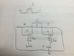
The switch can not be really turned off due to the drain-bulk and source bulk current.
The psub and drain or psub and source form the diodes, and pusb voltage is ground.
When switch is off( gate voltage is 0), the two diodes are reversely biased, but there is still some tiny current going through the reversely biased diodes. Say if the voltage of drain and source is 0.5V and 0.6V, then Vdb=0.5V, Vsb=0.6V, the current going from drain to bulk or from source to bulk is sub-pA range.
How to minimize the leakage current? Any switch architecture help? Thanks.
