Continue to Site

Welcome to EDAboard.com

Welcome to our site! EDAboard.com is an international Electronics Discussion Forum focused on EDA software, circuits, schematics, books, theory, papers, asic, pld, 8051, DSP, Network, RF, Analog Design, PCB, Service Manuals... and a whole lot more! To participate you need to register. Registration is free. Click here to register now.

RAM description in vhdl

Status
Not open for further replies.
I've made a dual port ram (I hope):
component:
Code:
---------------------------------------------------------------------------------------------
-- Company: CEA                                                                            --
-- Engineer: Romain Michard  -   romain.michard@cea.fr                                     --
-- Create Date:    10/03/2016                                                              --
-- Module Name:    ram_mem                                                                 --
-- Project Name:   SEEL- PROJECT " Smart Sensor"                                           --
-- Additional Comments:                                                                    --
-- This module is a memory ram.                                                            --
---------------------------------------------------------------------------------------------
library ieee; 
use ieee.std_logic_1164.all;
use ieee.numeric_std.all;

entity ram_mem is 
  generic (
    data_size : integer:=12;
    address_size : integer:=2 
    );
  port(
    clock : in std_logic;
    enable_write : in std_logic; 
    enable_read : in std_logic; 
    address : in std_logic_vector (address_size-1 downto 0);
    data_in : in std_logic_vector(data_size-1 downto 0);
    data_out : out std_logic_vector(data_size-1 downto 0)
    );
end ram_mem;

architecture RTL of ram_mem is 

  type data_ram is array (0 to 2**address_size-1) of std_logic_vector(data_size-1 downto 0);
  signal signal_ram : data_ram := (others => (others => '0'));

begin

  process(clock) 
  begin
    if rising_edge(clock) then
      if (enable_write = '1') then 
        signal_ram(to_integer(unsigned(address))) <= data_in;
      end if; 
    end if;
  end process;
  
  process(clock) 
  begin
    if rising_edge(clock) then
      if (enable_read = '1') then 
        data_out <= signal_ram(to_integer(unsigned(address)));
      end if; 
    end if;
  end process;

end RTL;
testbench:
Code:
library ieee; 
use ieee.std_logic_1164.all;
use ieee.numeric_std.all;

entity tb_mem is
end tb_mem;

architecture test of tb_mem is
	component ram_mem is
  generic(
    data_size : integer := 12;  
    address_size : integer := 2 
    );
  port(
    clock : in std_logic;
    enable_write : in std_logic; 
    enable_read : in std_logic; 
    address : in std_logic_vector (address_size-1 downto 0);
    data_in : in std_logic_vector(data_size-1 downto 0);
    data_out : out std_logic_vector(data_size-1 downto 0)
    );
	end component ram_mem;
		
  signal s_clock: std_logic := '0';
  signal s_enable_write : std_logic := '0';
  signal s_enable_read : std_logic := '0';
  signal s_data_in : std_logic_vector(11 downto 0) := (others => '0');
  signal s_data_out : std_logic_vector(11 downto 0) := (others => '0');
  signal s_address : std_logic_vector (1 downto 0);
  
begin
  
	comp : ram_mem
  generic map(
    data_size => 12,      -- pixel size
    address_size  => 2    -- row size
  )
	port map(	
    clock => s_clock,
    enable_write => s_enable_write,
    enable_read => s_enable_read,
    address => s_address,
    data_in => s_data_in,
    data_out => s_data_out
  );
  
  clock : process
  begin
    wait for 1 ns;
    s_clock <= not s_clock;
  end process;
  
  write : process
  begin
    wait for 8 ns;
      s_enable_write <= not s_enable_write;
  end process; 
   
  read : process
  begin
    wait for 7 ns;
      s_enable_read <= '1';
    wait for 1 ns;
      s_enable_read <= '0';
  end process;
  
  test_vectors : process
  begin
    wait for 14 ns;
    for i in 0 to 15 loop
      s_address <= std_logic_vector(to_unsigned(15-i, 2));
      s_data_in <= std_logic_vector(to_unsigned(15-i, 12));
      wait for 8 ns;
    end loop;
    wait;
  end process;
  
end test;
and here is the result:

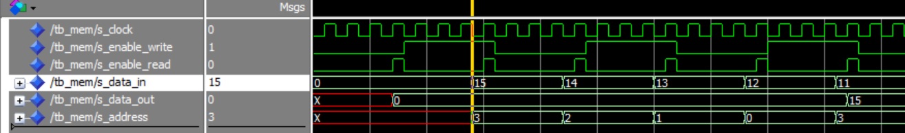
why is data_out ok after 32ns?
 

Not using clocked processes in your testbench is making your testbench a test of the simulators delta cycle handling.

Capture.JPG

As you can see the clock edge that the enable goes high is the same clock edge that causes the data to change, this might make you think that the data immediately comes out when you enable the output. It doesn't, it does this because you modeled the the interface incorrectly.
Code:
[FONT=Courier New]
   __    __    __    __    __    __   __
__|  |__|  |__|  |__|  |__|  |__|  |_|
          _____
_________/     \__________
        ^^    ^
        ||    |
        ||    `clk edge that detects the enable
        |`enable (generated from clk edge)
        `clk edge
[/FONT]
This delta cycle stuff is also why so many people (IMO less than stellar engineers) feel the need to add delays to every signal so they can see the signals transition somewhere other than the clock edges. I've seen it done in both testbench (which is okay for the most part) and in their RTL code :roll:.

- - - Updated - - -

The code generates a ram with a registered data_out.
Your new code just removes that register.
Why are you recommending such a change? you're advocate an asynchronous read ram (which will not infer a ram).

In any case this is not RAM. Just for the improper data he's reading, i proposed that code. If you need synchronous read he should have another clocked read and enable_read - where he should assign signal to data_out .
BTW, the code doesn't generate RAM, just few FFs.

Actually the RAM inputs are registered in both Xilinx and Altera. The output is asynchronous unless you add a register to the output data path. That is why the RAMs have a single clock cycle delay on reads, if you add a output FF you will end up with two clock cycles to get your read data, which is what is happening in the OPs case. Removing the register results in a synthesizable RAM with a single clock cycle read delay. Take a look at the blog post I gave in post #3. Of course there may be an issue with making it a simple assignment instead of within a process.
 

I've made a dual port ram (I hope):

Nope - this is a single port ram as it can only read or write on any given clock cycle.
A dual port ram can read and write on the same clock (simple dual port), or dual read or dual write (true dual port ram).
 

@ads-ee: just tell me how to make clocked processes in a testbench.
 

@ads-ee: just tell me how to make clocked processes in a testbench.

The same way you make a clocked process in RTL:


Code VHDL - [expand]
1
2
3
4
5
6
process(clk)
begin
  if rising_edge(clk) then
    --do something
  end if;
end process;


- - - Updated - - -

but you can do other things you cannot do in RTL also:


Code VHDL - [expand]
1
2
3
4
5
6
7
8
9
10
11
12
13
14
15
16
17
18
19
20
process  -- note no sensitivity list
begin
  ip <= '1';
  wait until rising_edge(clk);  -- single clock
 
  for i in 0 to 10 loop
    some_other_input(i) <= '1';
    wait until rising_edge(clk);
  end loop;  -- this waits for 11  clocks
 
  a <= 10;
 
  while there_is_no_output loop  -- indeterminate number of clocks
    wait until rising_edge(clk);
  end loop;
 
  finished_stimulus <= true;
 
  wait; -- halt the process
end process;


Everything seems ok. I hac a problem writing testbenches, not ram.
Thank you all.
 
  • Like
Reactions: ads-ee

    ads-ee

    Points: 2
    Helpful Answer Positive Rating
Status
Not open for further replies.

Part and Inventory Search

Welcome to EDABoard.com

Sponsor

Back
Top