Continue to Site

Welcome to EDAboard.com

Welcome to our site! EDAboard.com is an international Electronics Discussion Forum focused on EDA software, circuits, schematics, books, theory, papers, asic, pld, 8051, DSP, Network, RF, Analog Design, PCB, Service Manuals... and a whole lot more! To participate you need to register. Registration is free. Click here to register now.

[SOLVED] Processing an incoming stream of 8 bits data

Status
Not open for further replies.

dpaul

Advanced Member level 5
Joined
Jan 16, 2008
Messages
1,799
Helped
317
Reputation
635
Reaction score
342
Trophy points
1,373
Location
Germany
Activity points
13,069
Hello,

At a fixed clock rate, when an enable signal is high (at an interval of every 40ns), I have 8 bits data stream packs of the form (it is continuously being changed by the input source):
d5 5a 02 03 04 05 06
i.e. d5 is valid for 40ns, then 5a is valid for 40ns, and so on.

Now I want to convert this data stream in to the form:
05 0d 0a 05 02 00 03 00 04 00 05 00 06 00

Logically the split up would be that the LSB nibble of each 8 bits needs to be padded with "0000" and re transmitted as a separate 8 bit data. Then the MSB nibble of the same packet is to be padded with "0000" needs to be re-transmitted. That is to be repeated for all the incoming 8bit
1st split d5 --> 05 and then after 40ns d5 --> 0d. Then split 5a --> 0a and then 5a --> 05.

This split and transmission of the the new 8 bits should also happen when the same enable signal is high (at an interval of every 40ns). The clock will also remain the same.

What could be a clean and easy solution for this transformation.
 

I'm assuming as you are outputting twice as much data that you are buffering the input data in a FIFO or simple dual port RAM? Also that the input data is not continuous, as that would make the task impossible without running the output side at 2x the input clock.

I would read bytes from a FIFO and then the transformation of the nibbles into bytes is easily done using a simple daisy chain of nibble flip-flops. The upper bits don't need any registers they are just a constant 4'b0.


Code Verilog - [expand]
1
2
3
4
5
6
7
8
9
10
11
12
13
wire [7:0] my_byte; // from fifo
reg [3:0] my_lsn;
reg [3:0] my_msn;
wire [7:0] new_bytes;
 
always @(posedge clk) begin
  if (fifo_rd_q) begin
    {my_msn, my_lsn} <= my_byte; // loads the pipeline when the fifo gets read (done every other clock cycle)
  end else begin
    my_lsn <= my_msn; // update the lsn with the msn for second nibble
  end
end
assign new_bytes = {4'b0, my_lsn};


Add control logic, enables, and any extra registers to pipeline the output if necessary.
 
  • Like
Reactions: dpaul

    dpaul

    Points: 2
    Helpful Answer Positive Rating
What is the clock rate and how exactly does enable work? enables often have assumptions:
* an enable for one byte lasts for one cycle (not always true.)
* the byte is valid when valid is high (almost always true)
* if enable is low, the data is invalid. (sometimes the data will be forced to be the previously valid byte)

The endian issue is less interesting than the data doubling. You now have to send 2x data. If you have the following:

Code:
in:  d5 5a 02 03 04 05
out: 05 0d 0a 05 02 00
you can see there are problems.

if you have a higher rate clock, and can generate extra enables, then you can do something. Or if you can generate output enables when the input doesn't have them (and at sufficient rate) then you can do something.

You will likely need to generate an output enable. Many designs do this, where each module accepts an "data valid" input, and generate a new "data valid" output.

--edit:
also, unrelated, I didn't realize you could assign {x,y} <= z in Verilog. That makes me a little bit happier. thanks ads-ee
 
  • Like
Reactions: dpaul

    dpaul

    Points: 2
    Helpful Answer Positive Rating
I'm assuming as you are outputting twice as much data that you are buffering the input data in a FIFO or simple dual port RAM?

FIFO seems to be the way to go. I tried to find a solution without using FIFOs (using delayed versions of the signals or stuff like that...) but couldn't find a solution.I couldn't do much last night, investing a couple of hours, after a normal working day and after watching the EuroCup match between Spain and Turkey.

I will try out with FIFOs.

Thanks.


- - - Updated - - -
--------------------------------------------------------------------------------------------------------------------------------

What is the clock rate and how exactly does enable work? enables often have assumptions:
* an enable for one byte lasts for one cycle (not always true.)
* the byte is valid when valid is high (almost always true)
* if enable is low, the data is invalid. (sometimes the data will be forced to be the previously valid byte)
Clk is 125MHz (8ns), the 8bit data streams transitions after every for 40ns, i.e. 5x the clk. The enable goes HIGH once with the rising of the clk, once every 40ns, once for every 5 clk, pulse/enable duration being 8 ns.
An enable is asserted on the rising edge of the clock and then falls on the rising of the clk. Correct, the enable is not asserted for the entire 40ns data valid period.

if you have a higher rate clock, and can generate extra enables, then you can do something.
I always have the liberty to generate more frequent enables. That is possible and allowed! :)

Thanks.
 
Last edited:

At first sight, the answer seems trivial, not sure if I missed something.

It's clear that the output stream needs double the input data rate. If the clock rate is greater than 50 MHz (an input enable pulse is followed by at least one idle period), you can split the data without a FIFO.

Using regular synchronous logic, the first output strobe occurs one clock after the input strobe, the second one clock latter, possibly coinciding with the next input strobe.

A FIFO would be needed if the input rate can be temporarily faster than Fclk/2. The average rate must still keep this constraint.
 

Clk is 125MHz (8ns), the 8bit data streams transitions after every for 40ns, i.e. 5x the clk. The enable goes HIGH once with the rising of the clk, once every 40ns, once for every 5 clk, pulse/enable duration being 8 ns.
An enable is asserted on the rising edge of the clock and then falls on the rising of the clk. Correct, the enable is not asserted for the entire 40ns data valid period.


I always have the liberty to generate more frequent enables. That is possible and allowed! :)

Thanks.
This wasn't defined originally, this is very important. There is no need to use a FIFO at all if this description is what is being done.

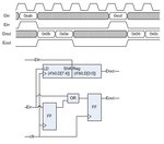
Something like this would do the trick.
Capture.JPG
Disclaimer, I haven't checked if this actually works, just drew the timing of what I would expect the input and output to look like and a quick circuit that should output the above waveform. The LD signal either loads if high or shifts otherwise.

As noted previously, you can leave out the 4'b0 as the output Dout[7:4] can just be connected directly to 0s.
 

Thanks ads-ee for your efforts on the diagram.
The problem is solved without the use of FIFOs.
 

Status
Not open for further replies.

Part and Inventory Search

Welcome to EDABoard.com

Sponsor

Back
Top