tiwari.sachin
Full Member level 6
Hello,
I am trying to communicate with RN4677 (Bluetooth Module from Microchip) from a Andriod device. We are having a issue with Bluetooth where
1. There is a delay in data reception (This happens randomly).
2. There probably is some data loss too (because of which I am getting some junk)
3. The signal strength is not that good (Works fine when the mobile is very close (less than half a meter) but have issues 1 and 2 when far.
I had two versions of PCB
1. First version was working relatively well.
2. Second version, I made some changes (did not touch Bluetooth section at all) but had the PCB done from another vendor. This version has more issues than the 1st. First was way too better.
I was using it for a thermal printer and noticed that the printer was sitting exactly above Bluetooth module (which has a metal casing) and this could be the problem.
So I decided to go with the new board design altogether. Here are the details
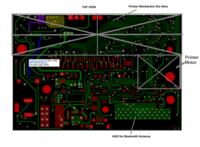
Above image is the TOP view of the PCB, the mechanism sits on the TOP side of the PCB (at rear) as shown
Also shown is the Grounding for Bluetooth.
The motor tends to heat up while continuous prints are given.
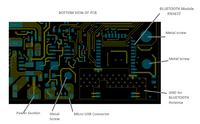
The image above shows the bottom view of the PCB where the Bluetooth sits and details of all the possible metal surrounding it.
There is no option to move the USB or screws as it has to fit the casing of the product.
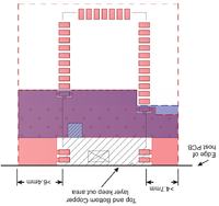
The above image gives the details of the suggested grounding for bluetooth which I have followed.
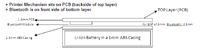
The above image gives details of how the PCB is placed in the casing.
Note: There is a Li Ion Battery that will sit below the bluetooth as I donot have space to place the bluetooth on TOP layer. Had to do it at bottom due to space constraint.
Are there any changes needed or am I doing it correctly.
Any suggestions on layout design shall be very helpful as we are having a few issues with connectivity and data transfer on previous boards.
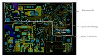
In the above image, you can see that I have placed the MCU and crystal (12Mhz) below the motor. As motor would heat up when there are continuous prints, this could probably effect the performance of the crystal.
Since there is no other space on PCB where I could use this, I somehow had to choose this as my final option.
I am not sure of the motor temperature when continuous prints are given but it does heat up a lot.
Am I placing the crystal in the right place and is the grounding around crystal correct?
I am trying to communicate with RN4677 (Bluetooth Module from Microchip) from a Andriod device. We are having a issue with Bluetooth where
1. There is a delay in data reception (This happens randomly).
2. There probably is some data loss too (because of which I am getting some junk)
3. The signal strength is not that good (Works fine when the mobile is very close (less than half a meter) but have issues 1 and 2 when far.
I had two versions of PCB
1. First version was working relatively well.
2. Second version, I made some changes (did not touch Bluetooth section at all) but had the PCB done from another vendor. This version has more issues than the 1st. First was way too better.
I was using it for a thermal printer and noticed that the printer was sitting exactly above Bluetooth module (which has a metal casing) and this could be the problem.
So I decided to go with the new board design altogether. Here are the details
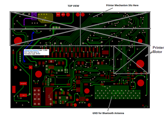
Above image is the TOP view of the PCB, the mechanism sits on the TOP side of the PCB (at rear) as shown
Also shown is the Grounding for Bluetooth.
The motor tends to heat up while continuous prints are given.
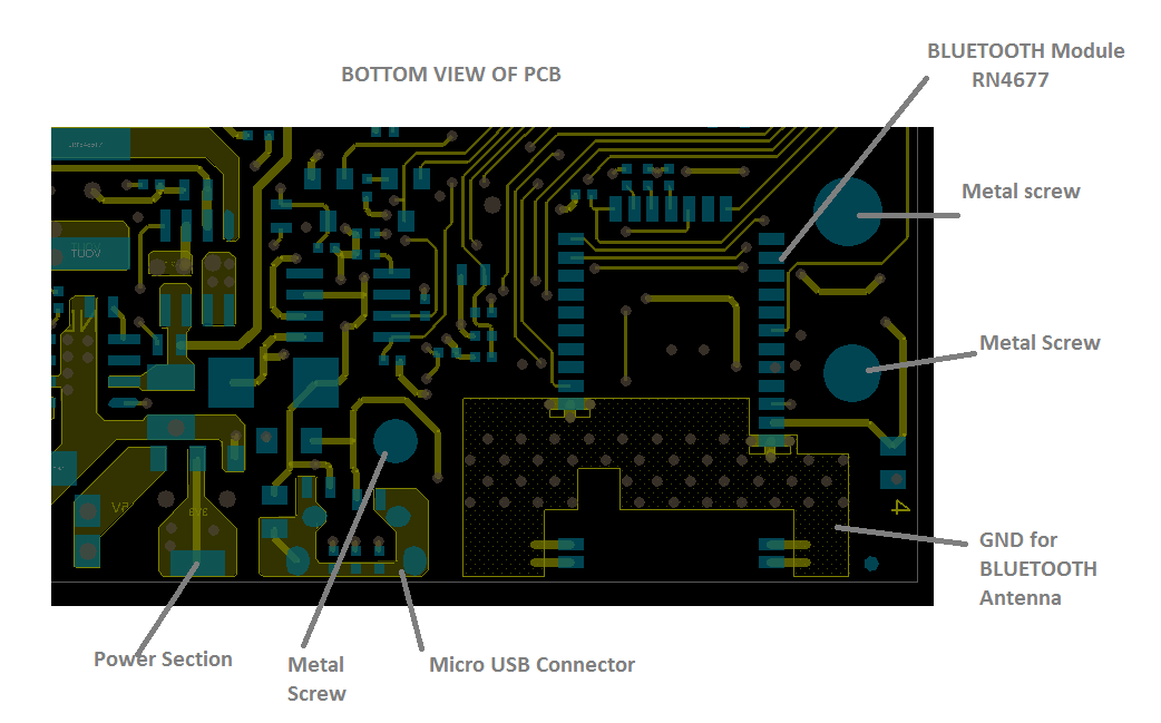
The image above shows the bottom view of the PCB where the Bluetooth sits and details of all the possible metal surrounding it.
There is no option to move the USB or screws as it has to fit the casing of the product.
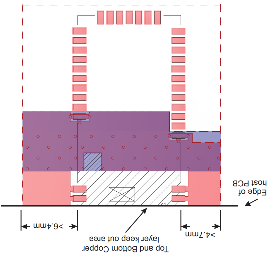
The above image gives the details of the suggested grounding for bluetooth which I have followed.
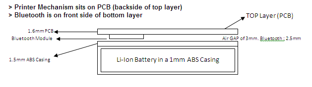
The above image gives details of how the PCB is placed in the casing.
Note: There is a Li Ion Battery that will sit below the bluetooth as I donot have space to place the bluetooth on TOP layer. Had to do it at bottom due to space constraint.
Are there any changes needed or am I doing it correctly.
Any suggestions on layout design shall be very helpful as we are having a few issues with connectivity and data transfer on previous boards.
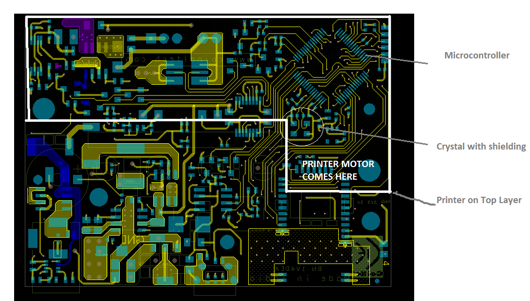
In the above image, you can see that I have placed the MCU and crystal (12Mhz) below the motor. As motor would heat up when there are continuous prints, this could probably effect the performance of the crystal.
Since there is no other space on PCB where I could use this, I somehow had to choose this as my final option.
I am not sure of the motor temperature when continuous prints are given but it does heat up a lot.
Am I placing the crystal in the right place and is the grounding around crystal correct?
