Continue to Site

Welcome to EDAboard.com

Welcome to our site! EDAboard.com is an international Electronics Discussion Forum focused on EDA software, circuits, schematics, books, theory, papers, asic, pld, 8051, DSP, Network, RF, Analog Design, PCB, Service Manuals... and a whole lot more! To participate you need to register. Registration is free. Click here to register now.

Push-pull PA test circuit (LDMOSFET)

Status
Not open for further replies.

ZHazami

Newbie level 5
Joined
Nov 9, 2015
Messages
8
Helped
0
Reputation
0
Reaction score
0
Trophy points
1
Activity points
87
Hi!

We have manufactured a PA test circuit with a LDMOSFET transistor (push-pull, two transistor in one package). during the DC test, by a small change in the bias voltage (Vgs) at one point, the current increases dramatically. this behavior happens for both transistor. We tried to test transistors and PCB separately by applying voltage of drain and gate at the bias point. We saw that during the test of the PCB, if we just apply voltage in one part of the circuit either input (Vgs) or output (VDS), we will have voltage in the other part. Regarding the test of transistors, knowing we have a broken transistor, we have normal behavior for both transistor of one package(zero voltage at one transistor when we apply voltage to the other).

Could anyone explain this action?
 

I would suspect the transistor is bursting into oscillations, and hence the sudden jump in operating point. Is there "hysteresis" in the DC current. i.e. when it suddenly turns on with a slight increase in voltage, does it stay on even if the voltage is reduced again?

you may be able to suppress oscillations with 50 ohm loads on input and output.
 

I agree with Biff44, you transistor is getting into oscillation and blowing itself off. did you consider unconditional stability at the start of the design across a wide bandwidth?
 

Thank you for the reply.
During the test we tried to increase and decrease the bias voltage. since we decrease the voltage it comes back to the stable state. It seems it works in on mode by reducing the bias voltage.

Thank you ahsoopk,
Actually this board is the test board of the transistor. And I think they have already considered the unconditional stability since they put some graphs in the datasheet with different Idq for power gain and efficiency.
 
Last edited by a moderator:

Thank you for the reply.
During the test we tried to increase and decrease the bias voltage. since we decrease the voltage it comes back to the stable state. It seems it works in on mode by reducing the bias voltage.

Thank you ahsoopk,
Actually this board is the test board of the transistor. And I think they have already considered the unconditional stability since they put some graphs in the datasheet with different Idq for power gain and efficiency.

Considering your design is a push pull type you might be using baluns or some sort of huge impedance transformers with huge transformation ratio. These things quickly run into oscillations if not taken care. Also, is there in any inductor chokes used in the bias line designs? What resistor values do you have across gate leads to bias lines?

Also, I will need check for the transconductance spread for both the transistors if you bias it from a single line.

Sure the device might have some issues, but in my experience it's always the PCB designs which causes issues.
 

Hi BMR,
Thank you for the reply.
Yes, you're right we have balun in our circuit. But the point is, we just did DC test without providing RF to PA.
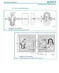
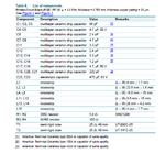
Yes, we have quarter wave microstrip functioning as a RF choke. you could see the schematic of the circuit and values of resistors in the attached images.

Regarding transconductance, by increasing the Vgs from 1.78V which is the for the bias to have 100 mA Idq, just a very small change, the current goes up to 2A.

Regards,
Zahra

2.png1.png
 

Yes, you're right we have balun in our circuit. But the point is, we just did DC test without providing RF to PA.
DC test shouldn't be a problem. But it must use 50 ohm termination of in- and outputs.
 

Hi FvM,

Thanks. we did the test of the board which you could find the results in the attached file.

22.png
11.png
 

Ok. Did you check your bias network configuration? Try changing the position of C4 and the shunt resistor. All it's values. Did you check if your bias network is configured to operate at Wc1 and Wc2?
Check for potential shorts in those areas.

My guess is if the transistor is turning on before reaching the threshold voltage then there is a short or a potential feedback, across the leads.

I suggest when performing DC IV measurements look through an IR cam to see hot spots. You should not see anything heating up at all. If some components are heating up then you know.
 
Last edited:

Status
Not open for further replies.

Part and Inventory Search

Welcome to EDABoard.com

Sponsor

Back
Top