Continue to Site

Welcome to EDAboard.com

Welcome to our site! EDAboard.com is an international Electronics Discussion Forum focused on EDA software, circuits, schematics, books, theory, papers, asic, pld, 8051, DSP, Network, RF, Analog Design, PCB, Service Manuals... and a whole lot more! To participate you need to register. Registration is free. Click here to register now.

LCRZ-Meter project(DDS signal source), large project with many questions/subjects.

Status
Not open for further replies.

David_

Advanced Member level 2
Joined
Dec 6, 2013
Messages
573
Helped
8
Reputation
16
Reaction score
8
Trophy points
1,308
Location
Sweden
Activity points
12,220
Hello.

This is the first post of a thread that will be running for a long time, though I can for see that I will erratically pop in and out but I am dead set on achieving the goal of this project so no matter how dead the thread may seem I will be back.

I can't give you all the details you would want because I don't know them my self yet, to begin with this thread will deal with a few system design problems much like my first question which will follow shortly(it ended up as kind of a long post).

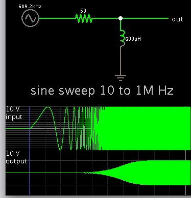
But I want to design a LCRZ-meter that will be connected through a isolated USB bus to a PC running Matlab(later a LCD shall be added to enable stand-alone operation but that is something that will be added when the meter is functional), the main feature of this meter is to be able to plot impedance vs frequency over a adjustable range(or something else vs frequency. But the maximum frequency range is going to be 10/50Hz up to 1MHz. I also have a ambition to enable a adjustable(and optional) DC-bias to be used to aces the DC currents effect on inductor cores and the DC voltages effect on ceramic capacitors.

Specifications(thus far):
Excitation Signal Frequency range: 50Hz(or 10Hz if there are any point in starting there) to 1MHz.
Excitation Signal Amplitude: 1Vp-p to 20Vp-p.
Excitation Signal Output Current: 1A(I suppose that would have to be ±1A).

The problem with that output current is that I want to make this a battery driven device, but at ebay they sell 3,7V Li-Ion AAA batteries with up to 10000mA/h and I don't mind having to use a few of those if that would enable my design to be run on batteries to be charged through USB(I can't plan for it but before this meter is done I am convinced that the USB C connector will have become the standard which means not 5V but 20V, and not 500mA but a few Watts)
Although I have begun discussing the battery situation in another thread so for now lets assume that I got the supply covered.

I have read as much as I can find on this subject, if I haven't been clear about it this meter shall function by using a DDS(AD9954) to generate a sine-wave, that sine-wave is amplified through a PGA/VGA stage and the current boosted some how before it is lead to the DUT.
Then I shall have 1 ADC to read the voltage developed over the DUT, and 1 ADC reading the voltage developed over a precision resistor that is in series with the DUT. The acquisition shall be performed in such a way that I can extrapolate the phase between these two signals, that is one major hurdle to overcome since I haven't figured out how that is done yet(I have begun studying complex numbers). I know that with these 3 peace's of information I can calculate everything from impedance to inductance to ESR, how that is done is a entirely different matter... But even though I may be hilariously far off from being able to do that I will not be able to rest in peace before I have learned to do it, and done it.

In any case I have thought to enable a user adjustable output voltage even if I am currently unsure about what that will give me, but being able to choose a 20Vp-p excitation signal has to to some extent enable the measurement of a smaller impedance, I think anyway, it sounds reasonable, as opposed to a maximum of 1,5Vp-p.

But do anyone have any objections or reasons to why I shouldn't use a large adjustable excitation signal amplitude?

I haven't considered how that will effect the acquisition hardware though, I mean I know I am in the need for a gain stage that can be switched between a number of gains, 1x, 10x, 100x & 1000x for example. But since the excitation voltage is so large I need to add a couple or even a few attenuation options as well...

But here comes my actual first question(the question which triggered this thread to be written, as you see there are lots of questions/subjects to cover):

I've got a Complete DDC IC(AD9954) as signal source, that IC has a differential current output(IOUT & -IOUT) and I have found this circuit(for the record it is the only one I have found so far but I have to think there are lots more out there):
DAC_differential_to_single-ended_converter.png

To this circuit came this text:
"The current output DAC drives balanced 25-Ω resistive loads, thereby developing an out-of-phase voltage of 0 to +0.5V at each output. This technique is used in lieu of a direct I/V conversion to prevent fast slewing DAC currents from overloading the amplifier and introducing distortion. Care must be taken so that the DAC output voltage is within its compliance rating.
The op-amp is configured for a gain of 2, to develop a final single-ended ground-referenced output voltage of 2-Vp-p. Note that because the output signal swings above and below ground, a dual-supply op amp is required."

But I feel a little insecure about this circuit, the AD9954's output DAC has a compliance voltage range of VDD - 0,5V to
VDD + 0,5V(the DAC is referenced to VDD rather than to GND).
Where VDD is +1,8V, and the combined output current is 15mA(max) and should be limited to 10mA to preserve the output specification/performance(done with a resistor appropriately chosen & connected to separate pin), but what does it mean that the combined output current is set to 10mA?
How do I choose the I/V resistors(the 25Ω resistors in the circuit above)?

Or am I right in thinking that I can do this?:
DAC_differential_to_single-ended_converter_for_AD9954.png
 

Specifications(thus far):
Excitation Signal Frequency range: 50Hz(or 10Hz if there are any point in starting there) to 1MHz.
Excitation Signal Amplitude: 1Vp-p to 20Vp-p.
Excitation Signal Output Current: 1A(I suppose that would have to be ±1A).
Reviewing the previous discussion, I guess you'll face serious difficulties to implement the intended specification. But everything at the proper time.

Regarding AD9954 DAC interface, things are simple. The DAC has a current source output, thus the output current doesn't depend on the load resistors, provided you keep the output voltage range. 2x 25 ohm have been chosen in the original application circuit to achieve 50 ohm differential output impedance. For your limited frequency range, a higher load impedance (e.g. 2 x 100 ohm) and respectively higher output level can be considered.
 
  • Like
Reactions: David_

    David_

    Points: 2
    Helpful Answer Positive Rating
Just to be clear, the goal of which I am dead set to achieve isn't a device with these specific specifications.
The realization of this meter as a hole is the goal, and I have no problem what so ever to change and make compromises.
The only specification which I am sure about is the frequency range, everything else is adaptable(I have just set up what I would wish was possible, but I am not interested in giving my self problems due to having to achieve some certain specification).

I don't know how I over looked it but TI has given out a 3-part application note called "Interfacing Op Amps to High-Speed DACs" , here you can find the first part: https://www.ti.com/lit/an/slyt342/slyt342.pdf which concerns current-sinking DACs. Part 2 is current-sourcing DACs.
This document appears to be spot on regarding what I need.

1, Sourcing/Sinking DAC?
But I can't find anything in the AD9954 datasheet regarding if it's DAC is sourcing or sinking current, is the fact that the DAC is referenced to VDD the only thing that tells me that the AD9954's DAC does sink current?(why do I think it means that the DAC sinks current? well I guessed... it's a 50/50 chance I'm right:))

In any case I have done so that I can easily adjust that particular op-amp to manage all possible situations, to be honest the above linked to app note does make my head hurt and I am in the process of fixing my mathematical skills(I have learned more about electronics without actually learning the math than I should have done so now I am studying mainly through https://www.mathtutordvd.com which is a really cool site where you can pay a small fee per month in order to get access to all there educational videos by streaming them and they offer lectures on all math subjects you could want(I think) and also some lecture series directly related to electronics and electronics engineering, I have been learning about KCL and KVL properly for the first time through buying an electronic engineering lecture series from that site, highly recommended to those whom want to learn) and right now I can't manage to go through this stage as I should(with the mathematical approach in the app note), but I am now sure about how it will look so I will leave the calculations for this stage for later and move on to other problems.

2, AD9954 pin voltage compliance protection?
I am now looking at what pins of the AD9954 should be connected to my microcontroller(AVR XMEGA) and some of the control pins does note that 1,8V is the maximum voltage that particular pin can be connected to(there are 3 power supplies in the AD9943, two +1,8V(AVDD & DVDD) and then there are a IO_DVDD which will run at 3,3V, and some pins demand a maximum equal to DVDD so the IO_DVDD 3,3V is too high) but I had though to connect 2 resistors and one 1,8V Zener diode to the control pins to be safe, 2 resistors?...
Well thinking about it I realized that I wasn't quite sure about the direction of influence on all pins and I thought that I should cover all situations by use a resistor from each direction before the Zener to cover all possibilities. I don't know it that is over kill and I don't know if others maybe favouring resistive dividers instead. The price of the AD9954 makes me extra vary of it's safety.
Illustration:
XMEGA_pin---resistor---|---resistor---AD9954_pin
|
zener
|
GND

3, the built in comparator?
Then about the built in comparator, the DDS(hence fort used instead of AD9954) has a COMP_IN & a -COMP_IN input pins, can those simply be connected to the same point that the DE-to-SE converter is connected to IOUT and -IOUT?
In order to output a square wave(on the COMP_OUT pin) at the same frequency that the sinewave is at, I will design the PCB so that I easily an solder on two jumpers to enable the comparator function in case I want/need to measure the DDS output frequency.

4, Output amplitude...
We are setting the maximum output current by connecting a resistor to a pin(DAC_Rset), so it is possible to make the output voltage amplitude adjustable by switching out the resistor for a digital potentiometer or DAC. On one hand that is a convenient solution but is it a proper solution...?
I don't know and I can't defend the following in a discussion but I think that it would be better to set the output current with a 1% resistor and leave the amplitude control to a stage further down the signal path, what do you think?

Maybe I don't even need to say it but I am in all cases interested in any thought or notes or ideas beside any answer to my questions, to bad I can't ask "how do you build a LCRZ-meter" and then someone would post a project with my specs:) but then it would be rather pointless since even though this project is one of those that I will use much when it is done the design and learning process is still a very big part of the project motivation.
But I have to confess that this project is close to above what I can handle, I like setting goals far over my head and force my self to learn but this project is different from others, seriously is the info on hoe to design a meter like this intentionally kept under wraps?
If anyone know of any info about a system in which the I and V and the phase is collected please tell me about it, the info about this is so scares so that I don't think it is possible for me to do this without edaboard.

5, System clock source
The XMEGA has a very versatile clock system but I think I really have no choice other than to use a external crystal because don't know why, (nor anything else about it) but what I know is that the DDS clock and ADC clock must adhere to some rules, do you know what they are?
I know it has something to do with the relation of clock frequency, I might be remembering incorrectly but the DDS frequency has to be higher than the ADC's.... No that doesn't sound correct, but it is important that they are not relatable to each other in some way, maybe integer multiple of each other just as there are a relationship between the DDS system clock and output frequency.

One important detail is that the technique I am still to understand enable ADC's with very low sample rates to be used even if the single frequency had a high frequency, oh how much I need to figure out...

Finely I just want to thank you all for all the help you have ever given to me and others, personally it results in a huge impact on my mental well-being to be able to have some place to ask for help.

Regards
 

Hi,

1, Sourcing/Sinking DAC?
But I can't find anything in the AD9954 datasheet regarding if it's DAC is sourcing or sinking current, is the fact that the DAC is referenced to VDD the only thing that tells me that the AD9954's DAC does sink current?

--> read:
* DAC OUTPUT CHARACTERISTICS
* "DAC Output" in the THEORY OF OPERATION section.
* IOUT in tabe 3
* see the EVALUATION BOARD SCHEMATICS

You are correct, it is not clearely stated.
Since the analog section is supplied with AVDD and the output should be biassed with a resistor to AVDD it is impossible to source current into this resistor.
(Else the IC needs an internal high voltage generation. But such a circuit generates noise... they surely try to avoid noise)

Klaus

- - - Updated - - -

added:

Now i found the missing information:

But the picture is named as "digital outputs"
(I´m surprised why "digital")
AD9954.PNG
--> only sinking against GND
 
1. The complementary DAC outputs are sinking current. Although there's no drawing of the output stage, you can conclude it from the specification.

2. Processor interface. AD9954 can perfectly work with a 3.3V processor when VDD_IO is set to 3.3V. I don't see a need for extra protection, but series resistors don't hurt.

4. Datasheet suggests to set the full scale output current between 5 and 15 mA. That doesn't give a large adjustment range. If you don't need the modulation feature, you can use the amplitude scale register to set the amplitude. For lowest distortion and best signal to noise ratio, a separate output attenuator should be used.
 
  • Like
Reactions: David_

    David_

    Points: 2
    Helpful Answer Positive Rating
2. Processor interface. AD9954 can perfectly work with a 3.3V processor when VDD_IO is set to 3.3V. I don't see a need for extra protection, but series resistors don't hurt.
PIN: 11
NAME: CLKMODESELECT
DESCRIPTION: Control Pin for the Oscillator Section
(1.8 V logic only). See REFCLK Input section for detailed instructions.

I can't tell what the practical results may be by adjusting the output current between 5 and 15mA(I don't know what the opamp circuit that reconfigures the output could yield in terms of maximum amplitude and that circuit situation is brand new for me and it is a quite weird one I think) or by adjusting the amplitude register(I first thought that that register could be used to control amplitude but then I read about it again and that time the text gave me an view of it as a function to adjust the amplitude but in a way that wouldn't be very helpful for me, to be clear I am not saying that that is the case)

Reviewing the previous discussion, I guess you'll face serious difficulties to implement the intended specification. But everything at the proper time.

Could we go into that a little deeper, I think you where referring to the output voltage range or the output current. Actually I think you where thinking of both those parameters, where you?

I have no way to tell at what range/level it becomes problematic, since you expressed it such as you did I would like to ask you(and hope it is an answerable question) if you could estimate a output voltage range/output current that wouldn't give me many problems?

I know that I don't have to have an adjustable signal voltage amplitude but I really want one, much because I need to have that in order to learn some things(I can't say more than that, everything is quite fussy in my mind right now)

I do see and agree that the most obvious solution is to use the AD9954's built in features(replacing resistor with DAC is considered internal here) but at the same time I can imaging that an external gain stage(or attenuator stage, in that case I would amplify the signal to the maximum I want in the DE-to-SE stage and then reduce that signal to gain the amplitude I want, I came up with that idea right now so I haven't thought it through).
I know here are a lot of IC's out there aimed at PGA/VGA functionality and I had hoped I could find a suitable IC or opamp + DAC/digi pot to enable a rather large voltage range for the signal.

I would be very grateful if you would expand on what is so difficult in the implementation and perhaps why?
Oh, I had made an assumption again here, could the serious difficulties be reduced by simply lowering the voltage range?
 

Hi,

I once did a measurement tool for test of piezo transducers.

I had a fixed frequency. 1MHz sine. I created it very clean with 4 PLD outputs and 4 analog switches. and some Rs and Cs. I think far below 1% distortion.

current sense with a shunt, OPAMP and a modified lock in amplifier...controlled with the same PLD.
low pass filter (to get DC) and a high resolution low frequency ADC (10 samples per second?)

--> capacitance resolution down to 100s of femtoFarads.
--> phase angle resolution far below 0.1 degree
--> very precise amplitude measurement far below 1%

To compensate for errors i did the measurement of U and I very symmetric.

After the hardware worked it took some effort to calibrate the existing errors: trace and wire impedance, lock in amplifier capacitance....

Klaus
 
Regarding clkmodeselect pin. It's unlikely that a design uses a crystal and external oscillator alternatively switched by microcontroller. The pin will be usually permanently connected to either or 1.8V. In so far no problem for a 3.3V processor interface.

"serious difficulties to implement the intended specification" referred to the combination of +/- 1A, 20 Vpp and 1MHz. It's not infeasible per se but probably not reasonable. Most signal generators will supply 1 MHz signal through a 50 ohm output matched amplifier. +/-1 A requires a low impedance voltage amplifier instead, not the first choice for wide band measurements. I think the output amplifier should be designed specifically for the impedance measurement circuit.
 
  • Like
Reactions: David_

    David_

    Points: 2
    Helpful Answer Positive Rating
Regarding clkmodeselect pin....

Of course, how silly of me not to consider a two-way solder jumper to set that pin.
If you hadn't mentioned that I would probably have continued on the path of "I have plenty of µC pins that isn't going to be used so why not control everything in software", but when I have come to writing the software I will no longer need to change that pin, unless I design in multiple options for driving the clock which I will not, probably.

I have come across some problems regarding the over all design of the system, I have read about the auto-balancing bridge which as far as I know is what I will use. But the documents talking about this says that such a bridge implemented with an opamp is only viable up to 100kHz and above that I really need to design a much more complex system with phase detector and mixers and other things I have heard of but never have known what they are made out of.

I am hoping that this information may be somewhat outdated such as there are today opamps I can use to go up to 1MHz, if not I have a big problem because I can't find any information relating to the other more complex system parts. Such as the needed phase detector, what is that made out of...?

Do anyone have any clues about this?
 

I just thought about something.

I will have a opamp circuit to convert the DDS output current to a voltage, then I thought to design a programmable gain stage to control the excitation signal amplitude.

But what about if I begin by amplifying the sine-wave to the maximum amplitude I would want and then implement some kind of programmable attenuator instead.

Does anyone have anything to say about that idea?

Regards
 

Hi,

Your (power) amplifier needs the gain setup for max. desirable output voltage.

With an EPOT or multiplying DAC you set the output amplitude from 0 to max.

Klaus
 
In my view, programmable gain and attenuator aren't an antagonism. Both are using switched resistors in case of doubt. In the RF range above e.g. several 100 MHz, you'll probably avoid variable gain stages, but they can be well implemented for 1 MHz.

There are several HP/Agilent documents describing their LCR meter auto-balancing method. See below an excerpt.

Related questions have been also discussed in this previous thread https://www.edaboard.com/threads/254201/
 

Attachments

  • 4284A Theory of Operation.pdf
    259.4 KB · Views: 111
  • Like
Reactions: David_

    David_

    Points: 2
    Helpful Answer Positive Rating
This post may be quite confused but I wrote a medium long post talking about a host of things but I manage to loose it, the auto-save system for when you are writing posts are one of my favourite features of this forum but it doesn't always work out very well.

Anyway, I don't think it is realistic for me to go with the more complex auto-balancing bridge design. It is simply too much to learn and it's hard to find info about it and it would be beneficial for my motivation if I choose the simple opamp auto-balancing bridge, I will look for and determine(to the best of my knowledge) the best opamp for this purpose.

I will try and think through the details my self but if anyone have any thoughts about the most important opamp characteristics I would very much like to know how you see this.


So on to the ADC, I will use 2 ADCs instead of 1 ADC multiplexed into 2 channels.
I where thinking about a 2 channel simultaneously sampling ADC but unless I recall incorrectly I think I read that such a ADC doesn't actually sample both channels at one and the same time, and if it doesn't then what would be the point of such a topology...?

One major hurdle that I seem to have forgot(or mistakenly thought that I had it figured out) is how to time the sampling with the DDS output waveform, I would like to perform under-sampling so that I can increase the performance of the ADC by running it at a slower speed. But I am not sure if that only goes for DC measurements(as a general rule of thumb) or if AC characteristics of ADCs also benefit from a slower sampling?

What I am unsure about is how does I time the sampling to ensure that I sample the wave something akin to this:

Sine_Wave_with_sample_points.png

In that picture I just happened to put the sampling-points with about 135° intervals.
But when doing under-sampling, how do I determine how often should I sample?

Since I am going to use frequency sweeps very often while doing measurements I want to spend as short a time a possible at each frequency while maintaining the highest resolution and accuracy that could be of use.
I have decided that the frequency range should be 10Hz to 1MHz but if I choose to sweep over that full range, how many different frequency's should I use to go from 10Hz up tp 1MHz...
What do you think about it?

I am not quite sure but I think my microcontroller will run at 48MHz(due to the µC's USB communication) and I will communicate with the ADC's through USART in Master SPI Mode(ordinary SPI does not support DMA's while USART in Master SPI Mode does support DMA's)

The DDS IC will convert the output sine-wave into a square-wave which is feed to the µC so that I can read the current frequency(which might be redundant since I was the one whom set the DDS frequency so I should already know what the output frequency is...)
But I will route the circuit as such in any case(but the comparator inputs needs to be fitted with two smd jumpers if the sine-wave is to reach them(I have ordered SMD jumpers, they are about 6.85mm and 0,97mm high and I think they can be really useful, there are others that are twice as long and other of the same length but with triple the hight)

The DDS IC does also feature a SYNC_OUT signal that I think is what I need to read with the µC and act upon in order to time the ADC sampling, the XMEGA has an event system which features a fixed time delay from the time that it is triggered to the time it's action is begun(it's kind of like an external interrupt) that happens over 3 clock cycles I think.

But the DDS is running at 400MHz/400MSPS and it is that clock that is outputted to the SYNC_OUT pin so I have to figure out some way of only acting upon every n SYNC pulses.

I have decided to make a PCB with the µC and the DDS as well as the DDS's I/V opamp converter, so that I can start write the software driver for the AD9954 and star experimenting with it, then later I'll make another board that connects to the first board.
 

I was going to ask for advice regarding how I determine the noise floor of the system, calculating the total system error and as said noise floor.

LM317 is apparently known for being noisy(partly deserved, partly not deserved) but I have been looking at low-noise regulators and there are some pretty quite stuff out there but as noise goes down the price goes up.

And I have been looking at "Active noise cancelling" circuits which takes the AC noise, inverts it and feeds it back to the power supply line to effectively cancel the noise.
But I don't know if I need it, although I could simply use one capacitance multiplier for each of the noise sensitive rails...

I do easily get confused while researching since I can't stay on one single subject and trying to read about 1 subject always results in hundreds of tabs with a hole host of subjects.

I know that noise sources are added together like this:
etot = sqrt(e12 + e22 + e32)
So that is no problem, but what part of the system will most likely determine the noise floor?
If I where to guess I would say the ADC/ADCs voltage reference but is it viable to look at the ADC/voltage reference and goes by that number?

I haven't even picked out a ADC yet since I don't quite grasp how the timing system is to be implemented but it might be that all I need is a ADC that can easily be controlled to perform single conversions so that I can trigger conversions from the DDS SYNC_OUT signal.
 

The next stage I need to get my head around is the stage(s) that controls the excitation signal amplitude, I am also thinking that this might be the location in the system for introducing a DC voltage.

I have begun looking at PGAs but those I have looked at thus far has been all wrong, but as I see it I need a PGA or multiple analog switches to switch in/out resistors.

I have been thinking about a high excitation signal amplitude(around 7-10Vpp)
and I don't really see the problem, not if I would only allow a certain number of different voltages spaced over a log scale.
What do you think about that?

I would however give my self problems in the ADC signal conditioning circuit, the higher the excitation voltage the more attenuation I need. I guess that I will need as many attenuation steps as I would have excitation amplitude steps that goes above the ADC reference voltage, and then I also need a gain stage something like 1x/10x/100x/1000x gain.
 

Somewhere you said you're taking your design from someone's working inductance meter project. This is good. Your plans are shaping up, and for all I know the project can do all you are asking of it. Nevertheless I can't help wondering if there isn't some crucial point where you'll encounter a bottleneck.

It is an interesting concept you mention, to apply DC and AC. You can detect ohmic resistance of the coil with DC, which is a parameter you want to know, of course.

I choose to sweep over that full range, how many different frequency's should I use to go from 10Hz up tp 1MHz...
What do you think about it?

First I would make jumps in multiples of 3 or 4x through the entire range, in a second or two. You want to find the general location of the rolloff curve. Then start a slower sweep in that narrower band.

The output forms the rolloff curve in the simulation. Notice the rolloff is obvious in a relatively narrow region of the sweep (about 1k to 30k Hz, for this LR combination). Your algorithm initially tests all frequencies, but it is for the purpose of ruling out the uninformative regions.

2956089300_1465197116.png


- - - Updated - - -

The uninformative regions are (a) 10 to 1k (all readings are near zero), and
(b) 30k to 1M (all readings are near maximum amplitude).
 
  • Like
Reactions: David_

    David_

    Points: 2
    Helpful Answer Positive Rating
Well I have a LCR_Meter design complete with Eagle CAD files and source code but the thing is that he who designed it did so to prove that he could design such a meter running of a single button battery(I don't know what they are called but they are on every PC motherboard I have ever seen).
So he's design is a single-supply design and he has done things to solve that situation which I don't even understand, but the point is that my design will be very different in both hardware and software.
I haven't written this person for a while but I have been composing a mail for past two days(formulating my thoughts about this project can be hard, here at edaboard I write about the easiest things to think about but other stuff gets really messy in my thoughts)

But I have only begun to feel as I am starting to get some kind of grip around this, for one thing I have read so much over such a time period that things have started to stick.
(did you know that people have tested and proved that there are a certain interval between the repetition of information that you should stick to in order to remember it, it's some thing like: read a text, read it again after 10min, read it again after 1 day, read it again after 1 week and finally read it again after one month(the only interval I can firmly remember is the after 10min interval, all the others are more a concept expressed).
The point is that this takes our brains memory storage into consideration and after you have repeated the information the last time is should be stored permanently. I often think about this ever since I listened to a documentary about it but I always forget about actually doing it:) )

Anyway I am not done in going through the system stages such that I can have an concept schematic but as I am going to use an auto-balancing bridge with a opamp the hardware seems surprisingly simple except for the probe configuration and the timing scheme between the DDS and ADC.
I will ask the person who designed that single cell LCR-Meter if a auto-balancing bridge will suffice, I don't know if it fits his algorithm which is the big thing I am gaining from he's design, he used some technique that meant:
a, I can use a slow speed ADC(undersampling).
b, common-mode noise is inherently eliminated.
c, errors are kept to a minimum
NOTE that this is very uncertain, all I can remember is that he explained the benefits of such an "topology" and it was something akin to what I wrote, I will re read all our emails and get back about that.

First I would make jumps in multiples of 3 or 4x through the entire range, in a second or two. You want to find the general location of the rolloff curve. Then start a slower sweep in that narrower band.
That sounds as a great idea, I wouldn't have thought about that for a long time if ever.
But there is something I don't like and I think that your suggestion is the clearly superior method but I am so confused about... well everything and I had envisioned and want to create x vs frequency plots in Matlab that has the same fine frequency resolution over the hole sweep. I think that has to do with how I would like to prove some things to me but I will definitely implement both and in the end I will probably do as you suggested as it's much more efficient. May be I'll be able to write some routine which does what you said but accepts inputs to tailor the algorithm with, then I could just sett everything to lets guess 0 and eliminate all the good ideas that would otherwise be implemented.

I have spent many hours now searching the net for solutions to my gain/attenuation problem and I am leaning towards the idea to first amplify the excitation signal to it's maximum and then switch a number or resistors in/out to result in the chosen amplitude.
A couple of problems though, even though I have read texts that said it was explained I still don't really grasp the role of the range setting resistor, which is also the current sensing resistor right?

First I was going to ask you about the attenuator because wouldn't that add a resistance in the signal path but I just realized that I'll put the attenuator before the final current boosting stage so a opamp is between the attenuator and the DUT.

Then we come to the question of attenuation, ether I use a IC with for example 8 to 1 analog multiplexer/switch and if I used 1 of those I could have 8 different amplitude settings as I connect the 1 port side of the IC to a resistor that leads to the signal source and the 8 other ports from the IC I tie 8 resistors to ground so I switch out the lower resistor in a voltage divider.

Or I can use some tiny MOSFET to allow a current carrying path to a resistor which connects to ground and then I simply add resistors that way in parallel to create the different amplitudes.

I had a couple of more ideas but I can't remember them now, it's funny, I begun writing this right after Brad posted his last post but it has taken some time to finish.
Oh man do I need to get a grip over this autism deal where one can sit for hours on end without being able to quite the task that one is doing, I waste countless hours searching online after things I don't need for the project.
 

I beleive I have found a solution for my power supply requirements, TI sells a part and in a project like mine it does not cost much at all. Its the TPS65131, it accepts a voltage between 2,7V and 5,5V and produces two adjustable rails, the positive rail can be adjusted between VIN+0,5V and +15V, while the negative rail can be adjusted to -15V to -2V and even though the part is advertised as being able to deliver 300mA Typ the specifications says 0,75A for ether rail.

The efficiency of the converter(s) is not so bad, at around 10mA its somewhere around 80% and at and above 100mA it rises to over 90%. And the input voltage range is set with Li-ion batteries in mind so I can build a 1 battery-pack with a 3,7V(4,2V-3V perhaps) and a lot of mA/h.

The circuit around the TPS65131 isn't complicated nor made out of many components and the inductor values it works with is between 3,3µH and 6,8µH.

does this sound viable?

I will make up a implementation for 750mA and quite low ripple voltage(and with filters to make it really silent.
I haven't decided yet but I'm thinking that maybe I should keep to ±5V rails.

Given that the package of TPS65131(VQFN-24) I can foresee problems with enabling 0,75A but I plan to use some rather unorthodox methods of mounting a heat-sink on top of the package kind of like those heat-sinks on PC motherboards that is hooked firmly to the board with small half circular pins, as well as giving it plenty of copper to dissipate heat through, if needed I can mount a small DC fan on the heat-sink.
 

Certain things are not at all clear.

The freq range: 10 Hz to 1MHz (this is fine)- but how you are planning to measure the impedance?

The freq amplitude: should be small- a 1V sine wave will be difficult to interpret. We usually use 10-100 mV modulation; See any commercial impedance machines...

The DC bias: Even a small DC bias can cause a large current and both the current and voltage must stay absolutely constant during the measurement; how?

Since you are planning a measurement over 5 decades, let us say 5 points over each decade- total of 5*5 points.

How many measurements at each point?

Are you planning to use the same technique for measurement at 10Hz and 1 MHz?
 

Certain things are not at all clear.
That is something of an understatement:)

The freq range: 10 Hz to 1MHz (this is fine)- but how you are planning to measure the impedance?
The impedance measurement is somewhat unclear to me, if we would look at the hole measurement system I haven't gotten further than to the point where I can adjust the excitation signal amplitude, I will soon show a schematic, I may be on the wrong path.

But without going into details I plan to measure the voltage from the DUT to ground, and then also measure the voltage from the range setting series resistor to ground and then simply take:
VR = VR_measured
VDUT = VDUT_measured - VR_measured

So that I don't need to bother with a differential measurement over the DUT.
Then I'll send those values to Matlab where I will manage all the other calculations to extrapolate the real, the imaginary and the phase value.

Now comes an uncertainty though, the schematic of the meter I have as a reference have a single series resistor and then adjusts the gain of the measurement signals, but I have not come across any such arrangement thus far in my readings.
The standard model used appears to be this(apart from my added circuit block, which is as far as I have gotten):
my_auto-balancing_bridge.png
And I had thought to switch out the Rr resistor with a few options as well.

The freq amplitude: should be small- a 1V sine wave will be difficult to interpret. We usually use 10-100 mV modulation; See any commercial impedance machines...
I clearly have to do that because I have a completely different idea, I was going to amplify my excitation signal to ±5V and then attenuate that with a number of different bottom resistors in a voltage divider.


The DC bias: Even a small DC bias can cause a large current and both the current and voltage must stay absolutely constant during the measurement; how?
I have thought to monitor the voltage over the Rr resistor, or over the DUT and use that as the input to a software control loop that will adjust the amplitude out of the DDS(I haven't solved this yet but even though there are a few amplifiers between the DDS and the DUT I am hoping that I can adjust the excitation signal through software through the DDS ICs amplitude register. If not then I have to rethink my complete circuit thus far.


How many measurements at each point?

Are you planning to use the same technique for measurement at 10Hz and 1 MHz?
I don't know the answer to ether of those questions yet, I haven't even picked out a ADC and I haven't designed the gain circuit that will come before the ADC in the signal chain.

It is much that I don't know and I have thought to make a PCB with the microcontroller, DDS with it's first I/V converting opamp(along with power supply) and the ADCs so that I can experiment with the parts I know I will need to have, then I can design another board with the signal conditioning circuits and the auto balancing bridge and the gain stages that is going to proceed the ADCs and I'll connect those boards together.

I know so little about DDS and this system so before I can get much further I feel that I need to have those first components to play with.
 

Status
Not open for further replies.

Part and Inventory Search

Welcome to EDABoard.com

Sponsor

Back
Top