Continue to Site

Welcome to EDAboard.com

Welcome to our site! EDAboard.com is an international Electronics Discussion Forum focused on EDA software, circuits, schematics, books, theory, papers, asic, pld, 8051, DSP, Network, RF, Analog Design, PCB, Service Manuals... and a whole lot more! To participate you need to register. Registration is free. Click here to register now.

Current Fed Push Pull Resonant Converter

Status
Not open for further replies.

fillherin

Newbie level 3
Joined
Apr 11, 2016
Messages
4
Helped
0
Reputation
0
Reaction score
0
Trophy points
1
Activity points
41
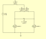
Hi, I am new to power electronics, this a push pull current fed converter.There is some part I do not understand, please help!!!!!
Capture.PNG

Let's consider there is no series resistance on inductors and capacitors. 1 of the switch is turning on and another one is turning off, both duty cycle is 50% and frequency of 100kHz.
The DC voltage source is 50V.
Capture.PNG
The red line is the voltage across L1, and Green line is the current of L1,
Question1: WHY THE CURRENT IS NEARLY ZERO? Actually it is around 0.0329 Amps(RMS), How do we calculate the L1 current?
Question2: WHY THE VOLTAGE GOES TO 50V(Maximum) and -30V(Minimum)? Why not -50V?


Thanks in advance!!:lol::lol::lol:
 

Schematic does not show the gate stimuli for the circuit.
Also your L2, L3 should be coupled inductors (xfmr) with
an output winding, bridge and inductor not shown. The
negative swing may have to do with the inductor not
being coupled to the opposite primary leg, its negative
clipping voltage may be the D-B diode of the FET
conducting (generally Not A Good Thing). The primary
should see swings between GND and V_DC*2 in a
voltage fed mode; what the L1 inductor does, I'm
unfamiliar with.

The near zero L1 current may be because there is no
energy taken off the system (secondary, load) so all
there is, is shuttling losses from switching the primary?
If everything is ideal-ish then a trivial input current
would be a normal outcome.

I think I'd start with the xfmr/bridge/load model and
the gate drive particulars. Make it as realistic and
application-appropriate as you can. Plot the two drain
voltages and the center tap point. Maybe that would
show some clues.
 

at least your sim results are correct, the problem here is that you do not have a good handle on how the ckt really works...
 

What is ckt, and how does it work?
 

Status
Not open for further replies.

Similar threads

Part and Inventory Search

Welcome to EDABoard.com

Sponsor

Back
Top