Continue to Site

Welcome to EDAboard.com

Welcome to our site! EDAboard.com is an international Electronics Discussion Forum focused on EDA software, circuits, schematics, books, theory, papers, asic, pld, 8051, DSP, Network, RF, Analog Design, PCB, Service Manuals... and a whole lot more! To participate you need to register. Registration is free. Click here to register now.

UCF for spi in nexys3

Status
Not open for further replies.
you need to look at the schematics and find which pins are connected to the uart and pmod connectors?? yes that all i want to knw to make the transfer from pc to 2fpga and back to fpga ?? can u help me how can i lock to schematic ??

actually i did uart code before and its works .. but uart its very easy .. the port are easy to put in ucf for nexys3 not like the spi

Ok... pmod connnectors are multi purpose I/O connectors. You can map any signal to them like SPI signals. Choose a connector like PmodA and map the spi clock to T12 pin in example.

Look at the page 21 of this document to know which pin you may choose. https://www.xilinx.com/support/docu... Boards/XUPNexys3/documentation/Nexys3_rm.pdf
 

i did that many times and it doesnt works with ,, i set before the pmod connector as mosi miso,sck ssel .. and i set the clk to clk in ucf ,, and rst to one of the button but nothing happen
 

i did that many times and it doesnt works with ,, i set before the pmod connector as mosi miso,sck ssel .. and i set the clk to clk in ucf ,, and rst to one of the button but nothing happen

See the following excerpt from the FORUM RULES:
Only you know what "doesn't work" means
Please tell us what your circuit or code is supposed to do and why it "doesn't work".When you come in and say "it doesn't work" or just "it has errors", that means NOTHING. There could be a million things wrong and no one will know where to look.

Show us what you've tried, i.e. post the entire UCF file you've tried for both sides of the design, where it doesn't work. Without that information we can only make guesses about what is wrong.
 

i did that many times and it doesnt works with ,, i set before the pmod connector as mosi miso,sck ssel .. and i set the clk to clk in ucf ,, and rst to one of the button but nothing happen

In your post #7, I see nowhere the pin used for the UART and the master clk and the reset. Please re-post the ucf with these information.
 

here is the spi master port

entity spi_master is
Generic (
N : positive := 32; -- 32bit serial word length is default
CPOL : std_logic := '0'; -- SPI mode selection (mode 0 default)
CPHA : std_logic := '0'; -- CPOL = clock polarity, CPHA = clock phase.
PREFETCH : positive := 2; -- prefetch lookahead cycles
SPI_2X_CLK_DIV : positive := 5); -- for a 100MHz sclk_i, yields a 10MHz SCK
Port (
sclk_i : in std_logic := 'X'; -- high-speed serial interface system clock
pclk_i : in std_logic := 'X'; -- high-speed parallel interface system clock
rst_i : in std_logic := 'X'; -- reset core
---- serial interface ----
spi_ssel_o : out std_logic; -- spi bus slave select line
spi_sck_o : out std_logic; -- spi bus sck
spi_mosi_o : out std_logic; -- spi bus mosi output
spi_miso_i : in std_logic := 'X'; -- spi bus spi_miso_i input
---- parallel interface ----
di_req_o : out std_logic; -- preload lookahead data request line
di_i : in std_logic_vector (N-1 downto 0) := (others => 'X'); -- parallel data in (clocked on rising spi_clk after last bit)
wren_i : in std_logic := 'X'; -- user data write enable, starts transmission when interface is idle
wr_ack_o : out std_logic; -- write acknowledge
do_valid_o : out std_logic; -- do_o data valid signal, valid during one spi_clk rising edge.
do_o : out std_logic_vector (N-1 downto 0); -- parallel output (clocked on rising spi_clk after last bit)
--- debug ports: can be removed or left unconnected for the application circuit ---
sck_ena_o : out std_logic; -- debug: internal sck enable signal
sck_ena_ce_o : out std_logic; -- debug: internal sck clock enable signal
do_transfer_o : out std_logic; -- debug: internal transfer driver
wren_o : out std_logic; -- debug: internal state of the wren_i pulse stretcher
rx_bit_reg_o : out std_logic; -- debug: internal rx bit
state_dbg_o : out std_logic_vector (3 downto 0); -- debug: internal state register
core_clk_o : out std_logic;
core_n_clk_o : out std_logic;
core_ce_o : out std_logic;
core_n_ce_o : out std_logic;
sh_reg_dbg_o : out std_logic_vector (N-1 downto 0) -- debug: internal shift register
);
end spi_master;

here is the ucf file for master

##Clock signal
Net "sclk_i" LOC=V10 | IOSTANDARD=LVCMOS33;
Net "sclk_i" TNM_NET = sys_clk_pin;
TIMESPEC TS_sys_clk_pin = PERIOD sys_clk_pin 100 mHz;

## Buttons
#Net "di_req_o" LOC = B8 | IOSTANDARD = LVCMOS33; #Bank = 0, pin name = IO_L33P, Sch name = BTNS
#Net "spi_miso_i" LOC = A8 | IOSTANDARD = LVCMOS33; #Bank = 0, pin name = IO_L33N, Sch name = BTNU
#Net "wren_i" LOC = C4 | IOSTANDARD = LVCMOS33; #Bank = 0, pin name = IO_L1N_VREF, Sch name = BTNL
Net "rst_i" LOC = C9 | IOSTANDARD = LVCMOS33; #Bank = 0, pin name = IO_L34N_GCLK18, Sch name = BTND
#Net "btn_i<4>" LOC = D9 | IOSTANDARD = LVCMOS33; # Bank = 0, pin name = IO_L34P_GCLK19, Sch name = BTNR


## 12 pin connectors

##JB
Net "spi_sck_o" LOC = K2 | IOSTANDARD = LVCMOS33; #Bank = 3, pin name = IO_L38P_M3DQ2, Sch name = JB1
Net "spi_ssel_o" LOC = K1 | IOSTANDARD = LVCMOS33; #Bank = 3, pin name = IO_L38N_M3DQ3, Sch name = JB2
Net "spi_mosi_o" LOC = L4 | IOSTANDARD = LVCMOS33; #Bank = 3, pin name = IO_L39P_M3LDQS, Sch name = JB3
#Net "spi_miso_i" LOC = L3 | IOSTANDARD = LVCMOS33; #Bank = 3, pin name = IO_L39N_M3LDQSN, Sch name = JB4
#Net "JB<4>" LOC = J3 | IOSTANDARD = LVCMOS33; #Bank = 3, pin name = IO_L40P_M3DQ6, Sch name = JB7
#Net "JB<5>" LOC = J1 | IOSTANDARD = LVCMOS33; #Bank = 3, pin name = IO_L40N_M3DQ7, Sch name = JB8
#Net "JB<6>" LOC = K3 | IOSTANDARD = LVCMOS33; #Bank = 3, pin name = IO_L42N_GCLK24_M3LDM, Sch name = JB9
#Net "JB<7>" LOC = K5 | IOSTANDARD = LVCMOS33; #Bank = 3, pin name = IO_L43N_GCLK22_IRDY2_M3CASN, Sch name = JB10

****i dont what signal that i will the uart rx tx in spi

here is spi slave port
entity spi_slave is
Generic (
N : positive := 32; -- 32bit serial word length is default
CPOL : std_logic := '0'; -- SPI mode selection (mode 0 default)
CPHA : std_logic := '0'; -- CPOL = clock polarity, CPHA = clock phase.
PREFETCH : positive := 3); -- prefetch lookahead cycles
Port (
clk_i : in std_logic := 'X'; -- internal interface clock (clocks di/do registers)
spi_ssel_i : in std_logic := 'X'; -- spi bus slave select line
spi_sck_i : in std_logic := 'X'; -- spi bus sck clock (clocks the shift register core)
spi_mosi_i : in std_logic := 'X'; -- spi bus mosi input
spi_miso_o : out std_logic := 'X'; -- spi bus spi_miso_o output
di_req_o : out std_logic; -- preload lookahead data request line
di_i : in std_logic_vector (N-1 downto 0) := (others => 'X'); -- parallel load data in (clocked in on rising edge of clk_i)
wren_i : in std_logic := 'X'; -- user data write enable
wr_ack_o : out std_logic; -- write acknowledge
do_valid_o : out std_logic; -- do_o data valid strobe, valid during one clk_i rising edge.
do_o : out std_logic_vector (N-1 downto 0); -- parallel output (clocked out on falling clk_i)
--- debug ports: can be removed for the application circuit ---
do_transfer_o : out std_logic; -- debug: internal transfer driver
wren_o : out std_logic; -- debug: internal state of the wren_i pulse stretcher
rx_bit_next_o : out std_logic; -- debug: internal rx bit
state_dbg_o : out std_logic_vector (3 downto 0); -- debug: internal state register
sh_reg_dbg_o : out std_logic_vector (N-1 downto 0) -- debug: internal shift register
);
end spi_slave;

here is the ucf for spi slave..

##Clock signal
Net "clk_i" LOC=V10 | IOSTANDARD=LVCMOS33;
Net "clk_i" TNM_NET = sys_clk_pin;
TIMESPEC TS_sys_clk_pin = PERIOD sys_clk_pin 100 mHz;

## Buttons
#Net "btns" LOC = B8 | IOSTANDARD = LVCMOS33; #Bank = 0, pin name = IO_L33P, Sch name = BTNS
Net "wren_i" LOC = A8 | IOSTANDARD = LVCMOS33; #Bank = 0, pin name = IO_L33N, Sch name = BTNU
Net "di_req_o" LOC = C4 | IOSTANDARD = LVCMOS33; #Bank = 0, pin name = IO_L1N_VREF, Sch name = BTNL
Net "wr_ack_o" LOC = C9 | IOSTANDARD = LVCMOS33; #Bank = 0, pin name = IO_L34N_GCLK18, Sch name = BTND
#Net "btnr" LOC = D9 | IOSTANDARD = LVCMOS33; # Bank = 0, pin name = IO_L34P_GCLK19, Sch name = BTNR


##JC
Net "spi_sck_i" LOC = H3 | IOSTANDARD = LVCMOS33; #Bank = 3, pin name = IO_L44N_GCLK20_M3A6, Sch name = JC1
Net "spi_ssel_i" LOC = L7 | IOSTANDARD = LVCMOS33; #Bank = 3, pin name = IO_L45P_M3A3, Sch name = JC2
Net "spi_mosi_i" LOC = K6 | IOSTANDARD = LVCMOS33; #Bank = 3, pin name = IO_L45N_M3ODT, Sch name = JC3
Net "spi_miso_o" LOC = G3 | IOSTANDARD = LVCMOS33; #Bank = 3, pin name = IO_L46P_M3CLK, Sch name = JC4
#Net "JC<4>" LOC = G1 | IOSTANDARD = LVCMOS33; #Bank = 3, pin name = IO_L46N_M3CLKN, Sch name = JC7
#Net "JC<5>" LOC = J7 | IOSTANDARD = LVCMOS33; #Bank = 3, pin name = IO_L47P_M3A0, Sch name = JC8
#Net "JC<6>" LOC = J6 | IOSTANDARD = LVCMOS33; #Bank = 3, pin name = IO_L47N_M3A1, Sch name = JC9
#Net "JC<7>" LOC = F2 | IOSTANDARD = LVCMOS33; #Bank = 3, pin name = IO_L48P_M3BA0, Sch name = JC10

thanks aloooot
 

How are these pairs of pins wired together? Are you using a custom cable or interface board between the two connectors? Need the schematic to determine if you have wired this up correctly.

Code:
------- SCK pair -------
#JB
Net "spi_sck_o" LOC = K2 | IOSTANDARD = LVCMOS33; #Bank = 3, pin name = IO_L38P_M3DQ2, Sch name = JB1
#JC
Net "spi_sck_i" LOC = H3 | IOSTANDARD = LVCMOS33; #Bank = 3, pin name = IO_L44N_GCLK20_M3A6, Sch name = JC1

------- SS pair -------
#JB
Net "spi_ssel_o" LOC = K1 | IOSTANDARD = LVCMOS33; #Bank = 3, pin name = IO_L38N_M3DQ3, Sch name = JB2
#JC
Net "spi_ssel_i" LOC = L7 | IOSTANDARD = LVCMOS33; #Bank = 3, pin name = IO_L45P_M3A3, Sch name = JC2

------- MOSI pair -------
#JB
Net "spi_mosi_o" LOC = L4 | IOSTANDARD = LVCMOS33; #Bank = 3, pin name = IO_L39P_M3LDQS, Sch name = JB3
#JC
Net "spi_mosi_i" LOC = K6 | IOSTANDARD = LVCMOS33; #Bank = 3, pin name = IO_L45N_M3ODT, Sch name = JC3

------- Unused N/C MISO pair -------
#JB
Net "spi_miso_o" LOC = G3 | IOSTANDARD = LVCMOS33; #Bank = 3, pin name = IO_L46P_M3CLK, Sch name = JC4
#JC
Net "spi_miso_i" LOC = L3 | IOSTANDARD = LVCMOS33; #Bank = 3, pin name = IO_L39N_M3LDQSN, Sch name = JB4
 

13187679_1066339290089072_961001570_n.jpg

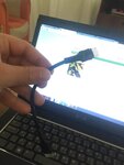
im goona use this cable from the connection between 2 fpga boards from pmod connector from fpga master to pmod connector slave fpga

- - - Updated - - -

and sir how can i show the schematic?
 

You draw your own schematic of the cable wiring using an ohm meter.

Are you sure you plugged the connector in correctly on both ends? A straight header connector can be easily plugged in backwards.

Capture.JPG
 

Yea im sure i did i connect the pmod connector in the right way
 

I don't have the time to teach you hands on debugging techniques, that is something that someone else can perhaps attempt, but it is something that is better if done by someone you know that is physically there with you.
 

Is the spi_master and spi_slave entities are both top_level? If so, there are a lot of signals that are not in the UCF. I noticed, that the spi_master has a pclk_i input. Is this signal is used in your code?

You are in a point that you need an oscilloscope to see if there's is a spi clock coming from the master and check if the signals are toggling. If not, you may need to use chipscope to probe internal signals to see the source of your error.

You may also map internal signals to other pmod connector and use the oscilloscope to debug.

From now, you need to get your hands dirty and learn how to debug.

Good luck.
 

actuallyy i have another code but i dont knw if i can use it betwwen two fpga? can u help me if it will work betwwen to fpga or not ?


Code VHDL - [expand]
1
2
3
4
5
6
7
8
9
10
11
12
13
14
15
16
17
18
19
20
21
22
23
24
25
26
27
28
29
30
31
32
33
34
35
36
37
38
39
40
41
42
43
44
45
46
47
48
49
50
51
52
53
54
55
56
57
58
59
60
61
62
63
64
65
66
67
68
69
70
71
72
73
74
75
76
77
78
79
80
81
82
83
84
85
86
87
88
89
90
91
92
93
94
95
96
97
98
99
100
101
102
103
104
105
106
107
108
109
110
111
112
113
114
115
116
117
118
119
120
121
122
123
124
125
126
127
128
129
130
131
132
133
134
135
136
137
138
139
140
141
142
143
144
145
146
147
148
149
150
151
152
153
154
155
156
157
158
159
160
161
162
163
164
165
166
167
168
169
170
171
172
173
174
175
176
177
178
179
180
181
182
183
184
185
186
187
188
189
190
191
192
193
194
195
196
197
198
199
200
201
202
203
204
205
206
207
208
209
210
211
212
213
214
215
216
217
218
219
220
221
222
223
224
225
226
227
228
229
230
231
232
233
234
235
236
237
238
239
240
241
242
243
244
245
246
247
248
249
250
251
252
253
254
255
256
257
258
259
260
261
262
263
264
265
266
267
268
269
270
271
272
273
274
275
276
277
278
279
280
281
282
283
284
285
286
287
288
289
290
291
292
293
294
295
296
297
298
299
300
301
302
303
304
305
306
307
308
309
310
311
312
313
314
315
316
317
318
319
320
321
322
323
324
325
326
327
328
329
330
331
332
333
334
335
336
337
338
339
340
341
342
343
344
345
346
347
348
349
350
351
352
353
354
355
356
357
358
359
360
361
362
363
364
365
366
367
368
369
370
371
372
373
374
375
376
377
378
379
380
381
382
383
384
385
386
387
388
389
390
391
392
393
394
395
396
397
398
399
400
401
402
403
404
405
406
407
408
409
410
411
412
413
414
415
416
417
418
419
420
421
422
423
424
425
426
427
428
429
430
431
432
433
434
435
436
437
438
439
440
441
442
443
444
445
446
447
448
449
450
451
452
453
454
455
456
457
458
459
460
461
462
463
464
465
466
467
468
469
470
471
472
473
474
475
476
477
478
479
480
481
482
483
484
485
486
487
488
489
490
491
492
493
494
495
496
497
498
499
500
501
502
503
504
505
506
507
508
509
510
511
512
513
514
515
516
517
518
519
520
521
522
523
524
525
526
527
528
529
530
531
532
533
534
535
536
537
538
539
540
541
542
543
544
545
546
547
548
549
550
551
552
553
554
555
556
557
558
559
560
561
562
563
564
565
566
567
568
569
570
571
572
573
574
575
576
577
578
579
580
581
582
583
584
585
586
587
588
589
590
591
592
593
594
595
library ieee;
use ieee.std_logic_1164.all;
use ieee.std_logic_arith.all;
 
entity spi_anan is
    Generic (   
        N : positive := 8;                              -- 8bit serial word length is default
        CPOL : std_logic := '0';                        -- SPI mode selection (mode 0 default)
        CPHA : std_logic := '0';                        -- CPOL = clock polarity, CPHA = clock phase.
        PREFETCH : positive := 3;                       -- prefetch lookahead cycles
        CLK_PERIOD : time := 10 ns;                     -- clock period for pclk_i (default 100MHz)
        DEBOUNCE_TIME : time := 2 us);                  -- switch debounce time (use 200 us for silicon, 2 us for simulation)
    Port (
        sclk_i : in std_logic := 'X';                   -- board clock input 100MHz
        pclk_i : in std_logic := 'X';                   -- board clock input 100MHz
        --- SPI interface ---           
        spi_ssel_o : out std_logic;                     -- spi port SSEL
        spi_sck_o : out std_logic;                      -- spi port SCK
        spi_mosi_o : out std_logic;                     -- spi port MOSI
        spi_miso_o: out std_logic;
 
          
        --- input slide switches ---            
        sw_i : in std_logic_vector (7 downto 0);        -- 8 input slide switches
        --- input buttons ---           
        btn_i : in std_logic_vector (5 downto 0);       -- 6 input push buttons
        --- output LEDs ----            
        led_o : out std_logic_vector (7 downto 0);      -- output leds
        --- debug outputs ---
        s_do_o : out std_logic_vector (7 downto 0);
        m_do_o : out std_logic_vector (7 downto 0);
        m_state_o : out std_logic_vector (3 downto 0);  -- master spi fsm state
        s_state_o : out std_logic_vector (3 downto 0);  -- slave spi fsm state
        dbg_o : out std_logic_vector (11 downto 0)      -- 12 generic debug pins
    );                      
end spi_anan;
 
architecture rtl of spi_anan is
 
    --=============================================================================================
    -- Constants
    --=============================================================================================
    -- clock divider count values from pclk_i (100MHz board clock)
    -- these constants shall not be zero
    constant FSM_CE_DIV         : integer := 1;     -- fsm operates at 100MHz
    constant SPI_2X_CLK_DIV     : integer := 1;     -- 50MHz SPI clock
    constant SAMP_CE_DIV        : integer := 1;     -- board signals sampled at 100MHz
    
    -- button definitions
    constant btRESET    : integer := 0;             -- these are constants to use as btn_i(x)
    constant btUP       : integer := 1;
    constant btLEFT     : integer := 2;
    constant btDOWN     : integer := 3;
    constant btRIGHT    : integer := 4;
    constant btCENTER   : integer := 5;
 
    --=============================================================================================
    -- Type definitions
    --=============================================================================================
    type fsm_master_write_state_type is 
            (st_reset, st_wait_spi_idle, st_wait_new_switch, st_send_spi_data_sw, st_wait_spi_ack_sw, 
            st_send_spi_data_1, st_wait_spi_ack_1, st_wait_spi_di_req_2, st_wait_spi_ack_2, 
            st_wait_spi_di_req_3, st_wait_spi_ack_3);
 
    type fsm_slave_write_state_type is 
            (st_reset, st_wait_spi_start, st_wait_spi_di_req_2, st_wait_spi_ack_2, st_wait_spi_do_valid_1,
            st_wait_spi_di_req_3, st_wait_spi_ack_3, st_wait_spi_end);
 
    type fsm_slave_read_state_type is
            (st_reset, st_wait_spi_do_valid_1, st_wait_spi_n_do_valid_1, st_wait_spi_do_valid_2, 
            st_wait_spi_n_do_valid_2, st_wait_spi_do_valid_3, st_wait_spi_n_do_valid_3);
 
    --=============================================================================================
    -- Signals for state machine control
    --=============================================================================================
    signal m_wr_st_reg  : fsm_master_write_state_type := st_reset;
    signal m_wr_st_next : fsm_master_write_state_type := st_reset;
    signal s_wr_st_reg  : fsm_slave_write_state_type := st_reset;
    signal s_wr_st_next : fsm_slave_write_state_type := st_reset;
    signal s_rd_st_reg  : fsm_slave_read_state_type := st_reset;
    signal s_rd_st_next : fsm_slave_read_state_type := st_reset;
 
    --=============================================================================================
    -- Signals for internal operation
    --=============================================================================================
    --- clock enable signals ---
    signal samp_ce          : std_logic := '1';         -- clock enable for sample inputs
    signal fsm_ce           : std_logic := '1';         -- clock enable for fsm logic
    --- switch debouncer signals ---
    signal sw_data          : std_logic_vector (7 downto 0) := (others => '0'); -- debounced switch data
    signal sw_reg           : std_logic_vector (7 downto 0) := (others => '0'); -- registered switch data 
    signal sw_next          : std_logic_vector (7 downto 0) := (others => '0'); -- combinatorial switch data
    signal new_switch       : std_logic := '0';                                 -- detector for new switch data
    --- pushbutton debouncer signals ---
    signal btn_data         : std_logic_vector (5 downto 0) := (others => '0'); -- debounced state of pushbuttons
    signal btn_reg          : std_logic_vector (5 downto 0) := (others => '0'); -- registered button data 
    signal btn_next         : std_logic_vector (5 downto 0) := (others => '0'); -- combinatorial button data
    signal new_button       : std_logic := '0';                                 -- detector for new button data
    --- spi port signals ---
    -- spi bus wires
    signal spi_ssel         : std_logic;
    signal spi_sck          : std_logic;
    signal spi_mosi         : std_logic;
    signal spi_miso         : std_logic;
    -- spi master port control signals
    signal spi_rst_reg      : std_logic := '1';
    signal spi_rst_next     : std_logic := '1';
    signal spi_ssel_reg     : std_logic;
    signal spi_wren_reg_m   : std_logic := '0';
    signal spi_wren_next_m  : std_logic := '0';
    -- spi master port flow control flags
    signal spi_di_req_m     : std_logic;
    signal spi_do_valid_m   : std_logic;
    -- spi master port parallel data bus
    signal spi_di_reg_m     : std_logic_vector (N-1 downto 0) := (others => '0');
    signal spi_di_next_m    : std_logic_vector (N-1 downto 0) := (others => '0');
    signal spi_do_m         : std_logic_vector (N-1 downto 0);
    signal spi_wr_ack_m     : std_logic;
    -- spi slave port control signals
    signal spi_wren_reg_s   : std_logic := '1';
    signal spi_wren_next_s  : std_logic := '1';
    -- spi slave port flow control flags
    signal spi_di_req_s     : std_logic;
    signal spi_do_valid_s   : std_logic;
    -- spi slave port parallel data bus
    signal spi_di_reg_s     : std_logic_vector (N-1 downto 0) := (others => '0');
    signal spi_di_next_s    : std_logic_vector (N-1 downto 0) := (others => '0');
    signal spi_do_s         : std_logic_vector (N-1 downto 0);
    signal spi_wr_ack_s     : std_logic;
    signal spi_rx_bit_s     : std_logic;
    -- spi debug data --
    signal spi_state_m      : std_logic_vector (3 downto 0);
    signal spi_state_s      : std_logic_vector (3 downto 0);
    -- slave data output regs --
    signal s_do_1_reg       : std_logic_vector (N-1 downto 0) := (others => '0');
    signal s_do_1_next      : std_logic_vector (N-1 downto 0) := (others => '0');
    signal s_do_2_reg       : std_logic_vector (N-1 downto 0) := (others => '0');
    signal s_do_2_next      : std_logic_vector (N-1 downto 0) := (others => '0');
    signal s_do_3_reg       : std_logic_vector (N-1 downto 0) := (others => '0');
    signal s_do_3_next      : std_logic_vector (N-1 downto 0) := (others => '0');
    -- other signals
    signal clear            : std_logic := '0';
    -- debug output signals
    signal leds_reg         : std_logic_vector (7 downto 0);
    signal leds_next        : std_logic_vector (7 downto 0) := (others => '0');
    signal dbg              : std_logic_vector (11 downto 0) := (others => '0');
begin
 
    --=============================================================================================
    -- COMPONENT INSTANTIATIONS FOR THE CORES UNDER TEST
    --=============================================================================================
    -- spi master port: data and control signals driven by the master fsm
    Inst_spi_master_port: entity work.spi_master(rtl) 
        generic map (N => N, CPOL => CPOL, CPHA => CPHA, PREFETCH => PREFETCH, SPI_2X_CLK_DIV => SPI_2X_CLK_DIV)
        port map( 
            sclk_i => sclk_i,                   -- system clock is used for serial and parallel ports
            pclk_i => pclk_i,
            rst_i => spi_rst_reg,
            spi_ssel_o => spi_ssel,
            spi_sck_o => spi_sck,
            spi_mosi_o => spi_mosi,
            spi_miso_i => spi_miso,             -- driven by the spi slave 
            di_req_o => spi_di_req_m,
            di_i => spi_di_reg_m,
            wren_i => spi_wren_reg_m,
            wr_ack_o => spi_wr_ack_m,
            do_valid_o => spi_do_valid_m,
            do_o => spi_do_m,
            ------------ debug pins ------------
            state_dbg_o => spi_state_m          -- debug: internal state register
        );
 
    -- spi slave port: data and control signals driven by the slave fsm
    Inst_spi_slave_port: entity work.spi_slave(rtl) 
        generic map (N => N, CPOL => CPOL, CPHA => CPHA, PREFETCH => PREFETCH)
        port map( 
            clk_i => pclk_i,
            spi_ssel_i => spi_ssel,             -- driven by the spi master
            spi_sck_i => spi_sck,               -- driven by the spi master
            spi_mosi_i => spi_mosi,             -- driven by the spi master
            spi_miso_o => spi_miso,
            di_req_o => spi_di_req_s,
            di_i => spi_di_reg_s,
            wren_i => spi_wren_reg_s,
            wr_ack_o => spi_wr_ack_s,
            do_valid_o => spi_do_valid_s,
            do_o => spi_do_s,
            ------------ debug pins ------------
            state_dbg_o => spi_state_s          -- debug: internal state register
        );                      
 
    -- debounce for the input switches, with new data strobe output
    Inst_sw_debouncer: entity work.grp_debouncer(rtl)
        generic map (N => 8, CNT_VAL => DEBOUNCE_TIME / CLK_PERIOD) -- debounce 8 inputs with selected settling time
        port map(  
            clk_i => pclk_i,                    -- system clock
            data_i => sw_i,                     -- noisy input data
            data_o => sw_data                   -- registered stable output data
        );
 
    -- debounce for the input pushbuttons, with new data strobe output
    Inst_btn_debouncer: entity work.grp_debouncer(rtl)
        generic map (N => 6, CNT_VAL => DEBOUNCE_TIME / CLK_PERIOD) -- debounce 6 inputs with selected settling time
        port map(  
            clk_i => pclk_i,                    -- system clock
            data_i => btn_i,                    -- noisy input data
            data_o => btn_data                  -- registered stable output data
        );
 
    --=============================================================================================
    --  CONSTANTS CONSTRAINTS CHECKING
    --=============================================================================================
    -- clock dividers shall not be zero
    assert FSM_CE_DIV > 0
    report "Constant 'FSM_CE_DIV' should not be zero"
    severity FAILURE;
    -- minimum prefetch lookahead check
    assert SPI_2X_CLK_DIV > 0
    report "Constant 'SPI_2X_CLK_DIV' should not be zero"
    severity FAILURE;
    -- maximum prefetch lookahead check
    assert SAMP_CE_DIV > 0
    report "Constant 'SAMP_CE_DIV' should not be zero"
    severity FAILURE;
 
    --=============================================================================================
    --  CLOCK GENERATION
    --=============================================================================================
    -- All registers are clocked directly from the 100MHz system clock.
    -- The clock generation block derives 2 clock enable signals, divided down from the 100MHz input 
    -- clock. 
    --      input sample clock enable, 
    --      fsm clock enable,
    -----------------------------------------------------------------------------------------------
    -- generate the sampling clock enable from the 100MHz board input clock 
    samp_ce_gen_proc: process (pclk_i) is
        variable clk_cnt : integer range SAMP_CE_DIV-1 downto 0 := 0;
    begin
        if pclk_i'event and pclk_i = '1' then
            if clk_cnt = SAMP_CE_DIV-1 then
                samp_ce <= '1';                 -- generate a single pulse every SAMP_CE_DIV clocks
                clk_cnt := 0;
            else
                samp_ce <= '0';
                clk_cnt := clk_cnt + 1;
            end if;
        end if;
    end process samp_ce_gen_proc;
    -- generate the fsm clock enable from the 100MHz board input clock 
    fsm_ce_gen_proc: process (pclk_i) is
        variable clk_cnt : integer range FSM_CE_DIV-1 downto 0 := 0;
    begin
        if pclk_i'event and pclk_i = '1' then
            if clk_cnt = FSM_CE_DIV-1 then
                fsm_ce <= '1';                  -- generate a single pulse every FSM_CE_DIV clocks
                clk_cnt := 0;
            else
                fsm_ce <= '0';
                clk_cnt := clk_cnt + 1;
            end if;
        end if;
    end process fsm_ce_gen_proc;
 
    --=============================================================================================
    -- INPUTS LOGIC
    --=============================================================================================
    -- registered inputs
    samp_inputs_proc: process (pclk_i) is
    begin
        if pclk_i'event and pclk_i = '1' then
            if samp_ce = '1' then
                clear <= btn_data(btUP);        -- clear is button UP
                leds_reg <= leds_next;          -- update LEDs with spi_slave received data
            end if;
        end if;
    end process samp_inputs_proc;
 
    --=============================================================================================
    --  REGISTER TRANSFER PROCESSES
    --=============================================================================================
    -- fsm state and data registers: synchronous to the system clock
    fsm_reg_proc : process (pclk_i) is
    begin
        -- FFD registers clocked on rising edge and cleared on sync 'clear'
        if pclk_i'event and pclk_i = '1' then
            if clear = '1' then                     -- sync reset
                m_wr_st_reg <= st_reset;            -- only provide local reset for the state registers
            else
                if fsm_ce = '1' then
                    m_wr_st_reg <= m_wr_st_next;    -- master write state register update
                end if;
            end if;
        end if;
        -- FFD registers clocked on rising edge and cleared on ssel = '1'
        if pclk_i'event and pclk_i = '1' then
            if spi_ssel = '1' then                  -- sync reset
                s_wr_st_reg <= st_reset;            -- only provide local reset for the state registers
                s_rd_st_reg <= st_reset;
            else
                if fsm_ce = '1' then
                    s_wr_st_reg <= s_wr_st_next;    -- slave write state register update
                    s_rd_st_reg <= s_rd_st_next;    -- slave read state register update
                end if;
            end if;
        end if;
        -- FFD registers clocked on rising edge, with no reset
        if pclk_i'event and pclk_i = '1' then
            if fsm_ce = '1' then
                --------- master write fsm signals -----------
                spi_wren_reg_m <= spi_wren_next_m;
                spi_di_reg_m <= spi_di_next_m;
                spi_rst_reg <= spi_rst_next;
                spi_ssel_reg <= spi_ssel;
                sw_reg <= sw_next;
                btn_reg <= btn_next;
                --------- slave write fsm signals -----------
                spi_wren_reg_s <= spi_wren_next_s;
                spi_di_reg_s <= spi_di_next_s;
                --------- slave read fsm signals -----------
                s_do_1_reg <= s_do_1_next;
                s_do_2_reg <= s_do_2_next;
                s_do_3_reg <= s_do_3_next;
            end if;
        end if;
    end process fsm_reg_proc;
 
    --=============================================================================================
    --  COMBINATORIAL NEXT-STATE LOGIC PROCESSES
    --=============================================================================================
    -- edge detector for new switch data
    new_switch_proc: new_switch <= '1' when sw_data /= sw_reg else '0';     -- '1' for change edge
 
    -- edge detector for new button data
    new_button_proc: new_button <= '1' when btn_data /= btn_reg else '0';   -- '1' for change edge
 
    -- master port write fsmd logic
    fsm_m_wr_combi_proc: process ( m_wr_st_reg, spi_wren_reg_m, spi_di_reg_m, spi_di_req_m, spi_wr_ack_m, 
                                spi_ssel_reg, spi_rst_reg, sw_data, sw_reg, new_switch, btn_data, btn_reg, 
                                new_button, clear) is
    begin
        spi_rst_next <= spi_rst_reg;
        spi_di_next_m <= spi_di_reg_m;
        spi_wren_next_m <= spi_wren_reg_m;
        sw_next <= sw_reg;
        btn_next <= btn_reg;
        m_wr_st_next <= m_wr_st_reg;
        case m_wr_st_reg is
            when st_reset =>
                spi_rst_next <= '1';                        -- place spi interface on reset
                spi_di_next_m <= (others => '0');           -- clear spi data port
                spi_wren_next_m <= '0';                     -- deassert write enable
                m_wr_st_next <= st_wait_spi_idle;
                
            when st_wait_spi_idle =>
                spi_wren_next_m <= '0';                     -- remove write strobe on next clock
                if spi_ssel_reg = '1' then
                    spi_rst_next <= '0';                    -- remove reset when interface is idle
                    m_wr_st_next <= st_wait_new_switch;
                end if;
 
            when st_wait_new_switch =>
                if new_switch = '1' then                    -- wait for new stable switch data
                    sw_next <= sw_data;                     -- load new switch data (end the mismatch condition)
                    m_wr_st_next <= st_send_spi_data_sw;
                elsif new_button = '1' then
                    btn_next <= btn_data;                   -- load new button data (end the mismatch condition)
                    if clear = '0' then
                        if btn_data(btDOWN) = '1' then
                            m_wr_st_next <= st_send_spi_data_sw;
                        elsif btn_data(btLEFT) = '1' then
                            m_wr_st_next <= st_send_spi_data_1;
                        elsif btn_data(btCENTER) = '1' then
                            m_wr_st_next <= st_send_spi_data_1;
                        elsif btn_data(btRIGHT) = '1' then
                            m_wr_st_next <= st_send_spi_data_1;
                        end if;
                    end if;
                end if;
            
            when st_send_spi_data_sw =>
                spi_di_next_m <= sw_reg;                    -- load switch register to the spi port
                spi_wren_next_m <= '1';                     -- write data on next clock
                m_wr_st_next <= st_wait_spi_ack_sw;
 
            when st_wait_spi_ack_sw =>                      -- the actual write happens on this state
                if spi_wr_ack_m = '1' then
                    spi_wren_next_m <= '0';                 -- remove write strobe on next clock
                    m_wr_st_next <= st_wait_spi_di_req_2;
                end if;
                
            when st_send_spi_data_1 =>
                spi_di_next_m <= X"A1";                     -- load switch register to the spi port
                spi_wren_next_m <= '1';                     -- write data on next clock
                m_wr_st_next <= st_wait_spi_ack_1;
 
            when st_wait_spi_ack_1 =>                       -- the actual write happens on this state
                if spi_wr_ack_m = '1' then
                    spi_wren_next_m <= '0';                 -- remove write strobe on next clock
                    m_wr_st_next <= st_wait_spi_di_req_2;
                end if;
                
            when st_wait_spi_di_req_2 =>
                if spi_di_req_m = '1' then
                    spi_di_next_m <= X"A2";
                    spi_wren_next_m <= '1';
                    m_wr_st_next <= st_wait_spi_ack_2;
                end if;
        
            when st_wait_spi_ack_2 =>                       -- the actual write happens on this state
                if spi_wr_ack_m = '1' then
                    spi_wren_next_m <= '0';                 -- remove write strobe on next clock
                    m_wr_st_next <= st_wait_spi_di_req_3;
                end if;
                
            when st_wait_spi_di_req_3 =>
                if spi_di_req_m = '1' then
                    spi_di_next_m <= X"A3";
                    spi_wren_next_m <= '1';
                    m_wr_st_next <= st_wait_spi_ack_3;
                end if;
 
            when st_wait_spi_ack_3 =>                       -- the actual write happens on this state
                if spi_wr_ack_m = '1' then
                    spi_wren_next_m <= '0';                 -- remove write strobe on next clock
                    m_wr_st_next <= st_wait_spi_idle;       -- wait transmission end
                end if;
                
            when others =>
                m_wr_st_next <= st_reset;                   -- state st_reset is safe state
                
        end case; 
    end process fsm_m_wr_combi_proc;
 
    -- slave port write fsmd logic
    fsm_s_wr_combi_proc: process (  s_wr_st_reg, spi_di_req_s, spi_wr_ack_s, spi_do_valid_s,
                                    spi_di_reg_s, spi_wren_reg_s, spi_ssel_reg) is
    begin
        spi_wren_next_s <= spi_wren_reg_s;
        spi_di_next_s <= spi_di_reg_s;
        s_wr_st_next <= s_wr_st_reg;
        case s_wr_st_reg is
            when st_reset =>
                spi_di_next_s <= X"51";                     -- write first data word
                spi_wren_next_s <= '1';                     -- set write enable
                s_wr_st_next <= st_wait_spi_start;
                
            when st_wait_spi_start =>
                if spi_ssel_reg = '0' then                  -- wait for slave select
                    spi_wren_next_s <= '0';                 -- remove write enable
                    s_wr_st_next <= st_wait_spi_di_req_2;
                end if;
 
            when st_wait_spi_di_req_2 =>
                if spi_di_req_s = '1' then
--                    spi_di_next_s <= X"D2";               -- do not write on this cycle (cycle miss)
--                    spi_wren_next_s <= '1';
--                    s_wr_st_next <= st_wait_spi_ack_2;
                    s_wr_st_next <= st_wait_spi_do_valid_1;
                end if;
        
            when st_wait_spi_ack_2 =>                       -- the actual write happens on this state
                if spi_wr_ack_s = '1' then
                    spi_wren_next_s <= '0';                 -- remove write strobe on next clock
                    s_wr_st_next <= st_wait_spi_di_req_3;
                end if;
                
            when st_wait_spi_do_valid_1 =>
                if spi_do_valid_s = '1' then
                    s_wr_st_next <= st_wait_spi_di_req_3;
                end if;
 
            when st_wait_spi_di_req_3 =>
                if spi_di_req_s = '1' then
                    spi_di_next_s <= X"D3";
                    spi_wren_next_s <= '1';
                    s_wr_st_next <= st_wait_spi_ack_3;
                end if;
 
            when st_wait_spi_ack_3 =>                       -- the actual write happens on this state
                if spi_wr_ack_s = '1' then
                    spi_wren_next_s <= '0';                 -- remove write strobe on next clock
                    s_wr_st_next <= st_wait_spi_end;        -- wait transmission end
                end if;
            
            when st_wait_spi_end =>                         -- wait interface to be deselected
                if spi_ssel_reg = '1' then
                    s_wr_st_next <= st_reset;               -- wait transmission start
                end if;
            
            when others =>
                s_wr_st_next <= st_reset;                   -- state st_reset is safe state
                
        end case; 
    end process fsm_s_wr_combi_proc;
 
    -- slave port read fsmd logic
    fsm_s_rd_combi_proc: process ( s_rd_st_reg, spi_do_valid_s, spi_do_s, s_do_1_reg, s_do_2_reg, s_do_3_reg) is
    begin
        s_do_1_next <= s_do_1_reg;
        s_do_2_next <= s_do_2_reg;
        s_do_3_next <= s_do_3_reg;
        s_rd_st_next <= s_rd_st_reg;
        case s_rd_st_reg is
            when st_reset =>
                s_rd_st_next <= st_wait_spi_do_valid_1;
                
            when st_wait_spi_do_valid_1 =>
                if spi_do_valid_s = '1' then                -- wait for receive data ready
                    s_do_1_next <= spi_do_s;                -- read data from output port
                    s_rd_st_next <= st_wait_spi_n_do_valid_1;
                end if;
 
            when st_wait_spi_n_do_valid_1 =>
                if spi_do_valid_s = '0' then
                    s_rd_st_next <= st_wait_spi_do_valid_2;
                end if;
        
            when st_wait_spi_do_valid_2 =>
                if spi_do_valid_s = '1' then                -- wait for receive data ready
                    s_do_2_next <= spi_do_s;                -- read data from output port
                    s_rd_st_next <= st_wait_spi_n_do_valid_2;
                end if;
 
            when st_wait_spi_n_do_valid_2 =>
                if spi_do_valid_s = '0' then
                    s_rd_st_next <= st_wait_spi_do_valid_3;
                end if;
        
            when st_wait_spi_do_valid_3 =>
                if spi_do_valid_s = '1' then                -- wait for receive data ready
                    s_do_3_next <= spi_do_s;                -- read data from output port
                    s_rd_st_next <= st_wait_spi_n_do_valid_3;
                end if;
                
            when st_wait_spi_n_do_valid_3 =>
                if spi_do_valid_s = '0' then
                    s_rd_st_next <= st_reset;
                end if;
 
            when others =>
                s_rd_st_next <= st_reset;                   -- state st_reset is safe state
                
        end case; 
    end process fsm_s_rd_combi_proc;
 
    leds_combi_proc: process (btn_data, leds_reg, s_do_1_reg, s_do_2_reg, s_do_3_reg) is
    begin
        leds_next <= leds_reg;
        if btn_data(btRIGHT) = '1' then
            leds_next <= s_do_3_reg;
        elsif btn_data(btCENTER) = '1' then
            leds_next <= s_do_2_reg;
        elsif btn_data(btLEFT) = '1' then
            leds_next <= s_do_1_reg;
        elsif btn_data(btDOWN) = '1' then
            leds_next <= s_do_1_reg;
        end if;
    end process leds_combi_proc;
 
    --=============================================================================================
    --  OUTPUT LOGIC PROCESSES
    --=============================================================================================
    -- connect the spi output wires
    spi_ssel_o_proc:        spi_ssel_o      <= spi_ssel;
    spi_sck_o_proc:         spi_sck_o       <= spi_sck;
    spi_mosi_o_proc:        spi_mosi_o      <= spi_mosi;
    spi_miso_o_proc:        spi_miso_o      <= spi_miso;
    -- connect leds_reg signal to LED outputs
    led_o_proc:             led_o           <= leds_reg;
 
    --=============================================================================================
    --  DEBUG LOGIC PROCESSES
    --=============================================================================================
    -- connect the debug vector outputs
    dbg_o_proc:             dbg_o <= dbg;
    
    -- connect debug port pins to spi ports instances interface signals
    -- master signals mapped on dbg
    dbg(11) <= spi_wren_reg_m;
    dbg(10) <= spi_wr_ack_m;
    dbg(9)  <= spi_di_req_m;
    dbg(8)  <= spi_do_valid_m;
    -- slave signals mapped on dbg
    dbg(7)  <= spi_wren_reg_s;
    dbg(6)  <= spi_wr_ack_s;
    dbg(5)  <= spi_di_req_s;
    dbg(4)  <= spi_do_valid_s;
    dbg(3 downto 0) <= spi_state_s;
    -- specific ports to test on testbench
    s_do_o <= spi_do_s;
    m_do_o <= spi_do_m;
    m_state_o <= spi_state_m;  -- master spi fsm state
    s_state_o <= spi_state_s;  -- slave spi fsm state
 
end rtl;


- - - Updated - - -

or if u have another codes for spi that can makes the transfer happen betwwen 2fpga and pc can u give it to me ?
 
Last edited by a moderator:

actuallyy i have another code but i dont knw if i can use it betwwen two fpga? can u help me if it will work betwwen to fpga or not ?
or if u have another codes for spi that can makes the transfer happen betwwen 2fpga and pc can u give it to me ?

The problem isn't because of which code you use. The root problem is you don't know how to design this. You've jumped right in with code and boards and builds and hardware and don't have a clue if any of the parts work. You probably don't even know what half the ports on the entity do.

If you want to design this.

Step 1. DRAW a block diagram of a design that does what you want, label all the interfaces, number of signals, the signal directions, what the signals are supposed to do, the various block and their function.
Step 2. For any block in the above diagram that does something complex, create another diagram or description of what is in that block so that it does what you specified in the top level block diagram. Repeat this step until you have blocks that you easily understand what they are supposed to do.
Step 3. Select how this "design" fits into you hardware. Assign pins and logic to the various parts of your hardware, if it doesn't fit then you need to go back to Step 1 until you have a design that both does what you want and fits in the hardware you have.
Step 4. Write the code that describes the complete design from Step 3.
Step 5. Verify the code from Step 4, using a simulator (much easier to do than testing on hardware). Iterate through Steps 1-4 depending on how "broken" the design is.
Step 6. Implement in vendor's tools, using correct timing constraints, iterate through Steps 1-5 depending on how poorly you met timing (e.g. you have ginormous comb circuits and want to run at 300 MHz).
Step 7. Download to FPGA board and do hardware verification tests and debugging. If you did a good job in steps 1-6 the design should just start working immediately, and any bugs will typically be unexpected corner cases.
 

Yesterday was a public holiday and so catching up now.........#33 posts and still no visible solution!

I would like to point out to the OP that hardware level debugging is very difficult in forums.
1st the OP was not sure about his UCF and now he thinks of using another RTL.
In my opinion this is not disciplined work.

Obviously he has ignored my advice in #12 of breaking the project into parts. The reply from ads-ee above, should help you more, if you follow it!
I had also shown him how to be specific about asking questions, but that was also ignored I guess.

It is not that I want to help, but in this particular case I will quit.
 
Last edited:

Hi,

@ OP:
to picture the problem:

You want to send a parcel to your friend.
(=You want to transmit data)

You select a parcel service
(=You select SPI on FPGA)

BUT you don´t tell the parcel service the address of your friend
(= you dont tell the compiler wich pins to use)

--> Your parcel will not be delivered to your friend
(= the data are not transmitted to the targed FPGA)

You try to change the parcel service
(you try to use another code)

--> this doesn´t help, because the new parcel service also doesn´t know where to deliver your parcel.
(a new code doesn´t help. You need to correctely assign the signals to the pins in the ucf)

Klaus
 

what i did in last 3 days ,, i broke the project into 3 parts .. the first part from master to pc .. i send data from master to pc but not the same data that i sent from pc ..

i tried with slave and fpga and it doesnt works..

i tried to make the transfer happen in 1 fpga also i can send data from fpga to pc but not same data that i sent from pc ..

im really want a help in ucf bucuz first of all im just bignner i can handle i simple project like uart on fpga but not like this code for spi its very complicated and there are alot of signals must be in the ucf to make the transfer happen betwen 2 fpga and pc ..

im really need a help in the ucf and im appreciate all ur helps till the end of my life.
thanks guys.
 

Hi,

what i did in last 3 days ,, i broke the project into 3 parts .. the first part from master to pc .. i send data from master to pc but not the same data that i sent from pc ..
Your posting has not arrived in the forum.
So please show us your work.

Klaus
 

im really want a help in ucf bucuz first of all im just bignner i can handle i simple project like uart on fpga but not like this code for spi its very complicated and there are alot of signals must be in the ucf to make the transfer happen betwen 2 fpga and pc ..

What makes you think that the problem is in the UCF?

From the code you posted in #25 for the master and the slave, there are a lot ports that must be connected to some user logic in the FPGA to control the cores. We haven't seen this code yet. I'm thinking that you only copy-pasted these codes and compiled them without any adaptation for your design/needs.
 

i posted before and i will post agian there..

----------------------------------------------------------------------------------

Code VHDL - [expand]
1
2
3
4
5
6
7
8
9
10
11
12
13
14
15
16
17
18
19
20
21
22
23
24
25
26
27
28
29
30
31
32
33
34
35
36
37
38
39
40
41
42
43
44
45
46
47
48
49
50
51
52
53
54
55
56
57
58
59
60
61
62
63
64
65
66
67
68
69
70
71
72
73
74
75
76
77
78
79
80
81
82
83
84
85
86
87
88
89
90
91
92
93
94
95
96
97
98
99
100
101
102
103
104
105
106
107
108
109
110
111
112
113
114
115
116
117
118
119
120
121
122
123
124
125
126
127
128
129
130
131
132
133
134
135
-- Company: 
-- Engineer: 
-- 
-- Create Date:    23:44:37 05/17/2011 
-- Design Name: 
-- Module Name:    spi_loopback - Behavioral 
-- Project Name: 
-- Target Devices: 
-- Tool versions: 
-- Description: 
--          This is a simple wrapper for the 'spi_master' and 'spi_slave' cores, to synthesize the 2 cores and
--          test them in the simulator.
--
-- Dependencies: 
--
-- Revision: 
-- Revision 0.01 - File Created
-- Additional Comments: 
--
----------------------------------------------------------------------------------
library ieee;
use ieee.std_logic_1164.all;
 
library work;
use work.all;
 
entity spi_loopback is
    Generic (   
        N : positive := 32;                                         -- 32bit serial word length is default
        CPOL : std_logic := '0';                                    -- SPI mode selection (mode 0 default)
        CPHA : std_logic := '1';                                    -- CPOL = clock polarity, CPHA = clock phase.
        PREFETCH : positive := 2;                                   -- prefetch lookahead cycles
        SPI_2X_CLK_DIV : positive := 5                              -- for a 100MHz sclk_i, yields a 10MHz SCK
        );                                  
    Port(
        ----------------MASTER-----------------------
        m_clk_i : IN std_logic;
        m_rst_i : IN std_logic;
        m_spi_ssel_o : OUT std_logic;
        m_spi_sck_o : OUT std_logic;
        m_spi_mosi_o : OUT std_logic;
        m_spi_miso_i : IN std_logic;
        m_di_req_o : OUT std_logic;
        m_di_i : IN std_logic_vector(N-1 downto 0);
        m_wren_i : IN std_logic;          
        m_do_valid_o : OUT std_logic;
        m_do_o : OUT std_logic_vector(N-1 downto 0);
        ----- debug -----
        m_do_transfer_o : OUT std_logic;
        m_wren_o : OUT std_logic;
        m_wren_ack_o : OUT std_logic;
        m_rx_bit_reg_o : OUT std_logic;
        m_state_dbg_o : OUT std_logic_vector(3 downto 0);
        m_core_clk_o : OUT std_logic;
        m_core_n_clk_o : OUT std_logic;
        m_sh_reg_dbg_o : OUT std_logic_vector(N-1 downto 0);
        ----------------SLAVE-----------------------
        s_clk_i : IN std_logic;
        s_spi_ssel_i : IN std_logic;
        s_spi_sck_i : IN std_logic;
        s_spi_mosi_i : IN std_logic;
        s_spi_miso_o : OUT std_logic;
        s_di_req_o : OUT std_logic;                                         -- preload lookahead data request line
        s_di_i : IN std_logic_vector (N-1 downto 0) := (others => 'X');     -- parallel load data in (clocked in on rising edge of clk_i)
        s_wren_i : IN std_logic := 'X';                                     -- user data write enable
        s_do_valid_o : OUT std_logic;                                       -- do_o data valid strobe, valid during one clk_i rising edge.
        s_do_o : OUT std_logic_vector (N-1 downto 0);                       -- parallel output (clocked out on falling clk_i)
        ----- debug -----
        s_do_transfer_o : OUT std_logic;                                    -- debug: internal transfer driver
        s_wren_o : OUT std_logic;
        s_wren_ack_o : OUT std_logic;
        s_rx_bit_reg_o : OUT std_logic;
        s_state_dbg_o : OUT std_logic_vector (3 downto 0)                   -- debug: internal state register
--      s_sh_reg_dbg_o : OUT std_logic_vector (N-1 downto 0)                -- debug: internal shift register
        );
end spi_loopback;
 
architecture Structural of spi_loopback is
begin
 
    --=============================================================================================
    -- Component instantiation for the SPI master port
    --=============================================================================================
    Inst_spi_master: entity work.spi_master(rtl)
        generic map (N => N, CPOL => CPOL, CPHA => CPHA, PREFETCH => PREFETCH, SPI_2X_CLK_DIV => SPI_2X_CLK_DIV)
        port map( 
            sclk_i => m_clk_i,                      -- system clock is used for serial and parallel ports
            pclk_i => m_clk_i,
            rst_i => m_rst_i,
            spi_ssel_o => m_spi_ssel_o,
            spi_sck_o => m_spi_sck_o,
            spi_mosi_o => m_spi_mosi_o,
            spi_miso_i => m_spi_miso_i,
            di_req_o => m_di_req_o,
            di_i => m_di_i,
            wren_i => m_wren_i,
            do_valid_o => m_do_valid_o,
            do_o => m_do_o,
            ----- debug -----
            do_transfer_o => m_do_transfer_o,
            wren_o => m_wren_o,
            wr_ack_o => m_wren_ack_o,
            rx_bit_reg_o => m_rx_bit_reg_o,
            state_dbg_o => m_state_dbg_o,
            core_clk_o => m_core_clk_o,
            core_n_clk_o => m_core_n_clk_o,
            sh_reg_dbg_o => m_sh_reg_dbg_o
        );
 
    --=============================================================================================
    -- Component instantiation for the SPI slave port
    --=============================================================================================
    Inst_spi_slave: entity work.spi_slave(rtl)
        generic map (N => N, CPOL => CPOL, CPHA => CPHA, PREFETCH => PREFETCH)
        port map(
            clk_i => s_clk_i,
            spi_ssel_i => s_spi_ssel_i,
            spi_sck_i => s_spi_sck_i,
            spi_mosi_i => s_spi_mosi_i,
            spi_miso_o => s_spi_miso_o,
            di_req_o => s_di_req_o,
            di_i => s_di_i,
            wren_i => s_wren_i,
            do_valid_o => s_do_valid_o,
            do_o => s_do_o,
            ----- debug -----
            do_transfer_o => s_do_transfer_o,
            wren_o => s_wren_o,
            wr_ack_o => s_wren_ack_o,
            rx_bit_next_o => s_rx_bit_reg_o,
            state_dbg_o => s_state_dbg_o
--            sh_reg_dbg_o => s_sh_reg_dbg_o
        );
 
end Structural;


thanks alot

- - - Updated - - -

and here is the original ucf for this code ..

Code:
#Created by Constraints Editor (xc6slx45t-csg484-3) - 2011/06/08
NET "m_spi_2x_clk_i" TNM_NET = m_spi_2x_clk_i;
TIMESPEC TS_m_spi_2x_clk_i = PERIOD "m_spi_2x_clk_i" 15 ns HIGH 50%;
NET "s_clk_i" TNM_NET = s_clk_i;
TIMESPEC TS_s_clk_i = PERIOD "s_clk_i" 8 ns HIGH 50%;
#Created by Constraints Editor (xc6slx45t-csg484-3) - 2011/06/08
NET "m_clk_i" TNM_NET = m_clk_i;
TIMESPEC TS_m_clk_i = PERIOD "m_clk_i" 8 ns HIGH 50%;
NET "s_spi_sck_i" TNM_NET = s_spi_sck_i;
TIMESPEC TS_s_spi_sck_i = PERIOD "s_spi_sck_i" 30 ns HIGH 50%;
NET "m_spi_sck_o_OBUF" TNM_NET = m_spi_sck_o_OBUF;
TIMESPEC TS_m_spi_sck_o_OBUF = PERIOD "m_spi_sck_o_OBUF" 30 ns HIGH 50%;
NET "Inst_spi_master/core_n_clk" TNM_NET = Inst_spi_master/core_n_clk;
TIMESPEC TS_Inst_spi_master_core_n_clk = PERIOD "Inst_spi_master/core_n_clk" 30 ns HIGH 50%;
INST "m_di_i<0>" TNM = m_di;
INST "m_di_i<1>" TNM = m_di;
INST "m_di_i<2>" TNM = m_di;
INST "m_di_i<3>" TNM = m_di;
INST "m_di_i<4>" TNM = m_di;
INST "m_di_i<5>" TNM = m_di;
INST "m_di_i<6>" TNM = m_di;
INST "m_di_i<7>" TNM = m_di;
INST "m_di_i<8>" TNM = m_di;
INST "m_di_i<9>" TNM = m_di;
INST "m_di_i<10>" TNM = m_di;
INST "m_di_i<11>" TNM = m_di;
INST "m_di_i<12>" TNM = m_di;
INST "m_di_i<13>" TNM = m_di;
INST "m_di_i<14>" TNM = m_di;
INST "m_di_i<15>" TNM = m_di;
INST "m_di_i<16>" TNM = m_di;
INST "m_di_i<17>" TNM = m_di;
INST "m_di_i<18>" TNM = m_di;
INST "m_di_i<19>" TNM = m_di;
INST "m_di_i<20>" TNM = m_di;
INST "m_di_i<21>" TNM = m_di;
INST "m_di_i<22>" TNM = m_di;
INST "m_di_i<23>" TNM = m_di;
INST "m_di_i<24>" TNM = m_di;
INST "m_di_i<25>" TNM = m_di;
INST "m_di_i<26>" TNM = m_di;
INST "m_di_i<27>" TNM = m_di;
INST "m_di_i<28>" TNM = m_di;
INST "m_di_i<29>" TNM = m_di;
INST "m_di_i<30>" TNM = m_di;
INST "m_di_i<31>" TNM = m_di;
TIMEGRP "m_di" OFFSET = IN 8 ns VALID 8 ns BEFORE "m_clk_i" RISING;
INST "m_spi_miso_i" TNM = m_miso;
INST "s_di_i<0>" TNM = s_di;
INST "s_di_i<1>" TNM = s_di;
INST "s_di_i<2>" TNM = s_di;
INST "s_di_i<3>" TNM = s_di;
INST "s_di_i<4>" TNM = s_di;
INST "s_di_i<5>" TNM = s_di;
INST "s_di_i<6>" TNM = s_di;
INST "s_di_i<7>" TNM = s_di;
INST "s_di_i<8>" TNM = s_di;
INST "s_di_i<9>" TNM = s_di;
INST "s_di_i<10>" TNM = s_di;
INST "s_di_i<11>" TNM = s_di;
INST "s_di_i<12>" TNM = s_di;
INST "s_di_i<13>" TNM = s_di;
INST "s_di_i<14>" TNM = s_di;
INST "s_di_i<15>" TNM = s_di;
INST "s_di_i<16>" TNM = s_di;
INST "s_di_i<17>" TNM = s_di;
INST "s_di_i<18>" TNM = s_di;
INST "s_di_i<19>" TNM = s_di;
INST "s_di_i<20>" TNM = s_di;
INST "s_di_i<21>" TNM = s_di;
INST "s_di_i<22>" TNM = s_di;
INST "s_di_i<23>" TNM = s_di;
INST "s_di_i<24>" TNM = s_di;
INST "s_di_i<25>" TNM = s_di;
INST "s_di_i<26>" TNM = s_di;
INST "s_di_i<27>" TNM = s_di;
INST "s_di_i<28>" TNM = s_di;
INST "s_di_i<29>" TNM = s_di;
INST "s_di_i<30>" TNM = s_di;
INST "s_di_i<31>" TNM = s_di;
TIMEGRP "s_di" OFFSET = IN 8 ns VALID 8 ns BEFORE "s_clk_i" RISING;
INST "s_spi_mosi_i" TNM = s_mosi;
INST "m_do_o<0>" TNM = m_do;
INST "m_do_o<1>" TNM = m_do;
INST "m_do_o<2>" TNM = m_do;
INST "m_do_o<3>" TNM = m_do;
INST "m_do_o<4>" TNM = m_do;
INST "m_do_o<5>" TNM = m_do;
INST "m_do_o<6>" TNM = m_do;
INST "m_do_o<7>" TNM = m_do;
INST "m_do_o<8>" TNM = m_do;
INST "m_do_o<9>" TNM = m_do;
INST "m_do_o<10>" TNM = m_do;
INST "m_do_o<11>" TNM = m_do;
INST "m_do_o<12>" TNM = m_do;
INST "m_do_o<13>" TNM = m_do;
INST "m_do_o<14>" TNM = m_do;
INST "m_do_o<15>" TNM = m_do;
INST "m_do_o<16>" TNM = m_do;
INST "m_do_o<17>" TNM = m_do;
INST "m_do_o<18>" TNM = m_do;
INST "m_do_o<19>" TNM = m_do;
INST "m_do_o<20>" TNM = m_do;
INST "m_do_o<21>" TNM = m_do;
INST "m_do_o<22>" TNM = m_do;
INST "m_do_o<23>" TNM = m_do;
INST "m_do_o<24>" TNM = m_do;
INST "m_do_o<25>" TNM = m_do;
INST "m_do_o<26>" TNM = m_do;
INST "m_do_o<27>" TNM = m_do;
INST "m_do_o<28>" TNM = m_do;
INST "m_do_o<29>" TNM = m_do;
INST "m_do_o<30>" TNM = m_do;
INST "m_do_o<31>" TNM = m_do;
#Created by Constraints Editor (xc6slx45t-csg484-3) - 2011/06/09
INST "m_rx_bit_reg_o" TNM = m_rx_bit;

- - - Updated - - -

is it possible if i used uartcable and sent from hypeterminal word like " hello " master fpga recive and send to slave fpga then slave will send it back to pc ??
 
Last edited by a moderator:

is it possible if i used uartcable and sent from hypeterminal word like " hello " master fpga recive and send to slave fpga then slave will send it back to pc ??

From the code above, there's no chance. The uart pins are not mapped on the top module.

Do you realize that the code you posted is for simulation? Did you ever simulated it before?

I will ask as the other members of this forum asked. Post the block diagram of your design. We want to see the UART block with its interfaces. This UART must be connected to some user logic block i suppose and then this block connected to the spi core.
 

Status
Not open for further replies.

Part and Inventory Search

Welcome to EDABoard.com

Sponsor

Back
Top