Continue to Site

Welcome to EDAboard.com

Welcome to our site! EDAboard.com is an international Electronics Discussion Forum focused on EDA software, circuits, schematics, books, theory, papers, asic, pld, 8051, DSP, Network, RF, Analog Design, PCB, Service Manuals... and a whole lot more! To participate you need to register. Registration is free. Click here to register now.

Simple Counter using CD40192BE to LATCH TO 7 SEGMENT (CD4511BE)

Status
Not open for further replies.

wfg42438

Member level 3
Joined
Jun 29, 2015
Messages
54
Helped
0
Reputation
0
Reaction score
0
Trophy points
6
Location
California
Activity points
620
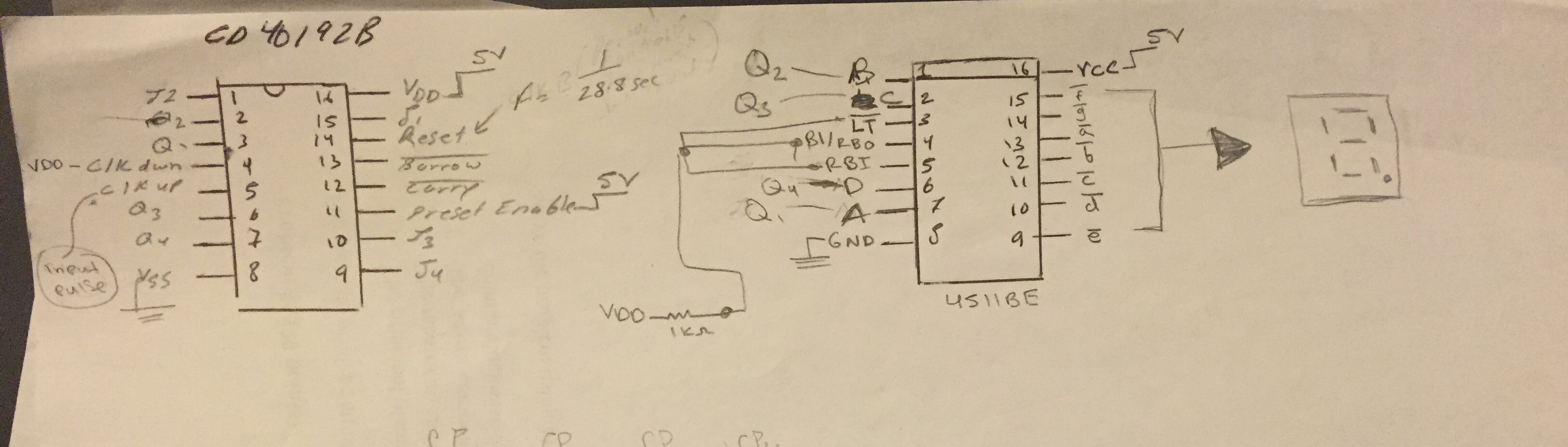
Hello I am attempting to set up three cascaded counters each going to BCD decoders and then to seven segment displays. i have one low frequency clock being applied to the clock up signal which i am attempting to count. An additional clock is also being used for the reset line of all counters. Please note that the input clock is a low frequency signal of approximately 1-35 Hz, and i wish to have the other clock reset the counter every 28.8 seconds so this clock has a frequency of 34.72mhz.

Please note that for now the clock signals have been given logic high levels of 5V and a logic low of 0V


You might be wondering why i want to set up such a slow and odd counter well this is for a project iam working on which is well described in this thread: https://www.edaboard.com/threads/353222/#post1512642

A much better solution has already been proposed but i am really curios to see how this counter works before i attempt the proper solution in the thread above.

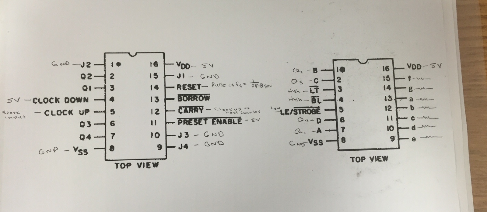
Now for the counters i wish to use the count up function therefore i have held Enable, and count down high by applying VDD (5V) as specified in the data sheet

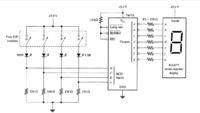
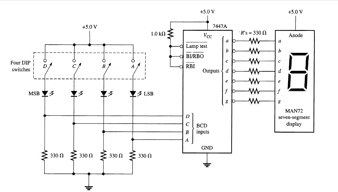
For the decoders i was not too sure about the connection scheme so i looked over an old digital logic lab book and saw the connection scheme attached. Please note i have used the 330 ohm resistors at the output of the decoder and the 1k resistor with one end to VDD and the other tied to LT, BI/RBO & RBI

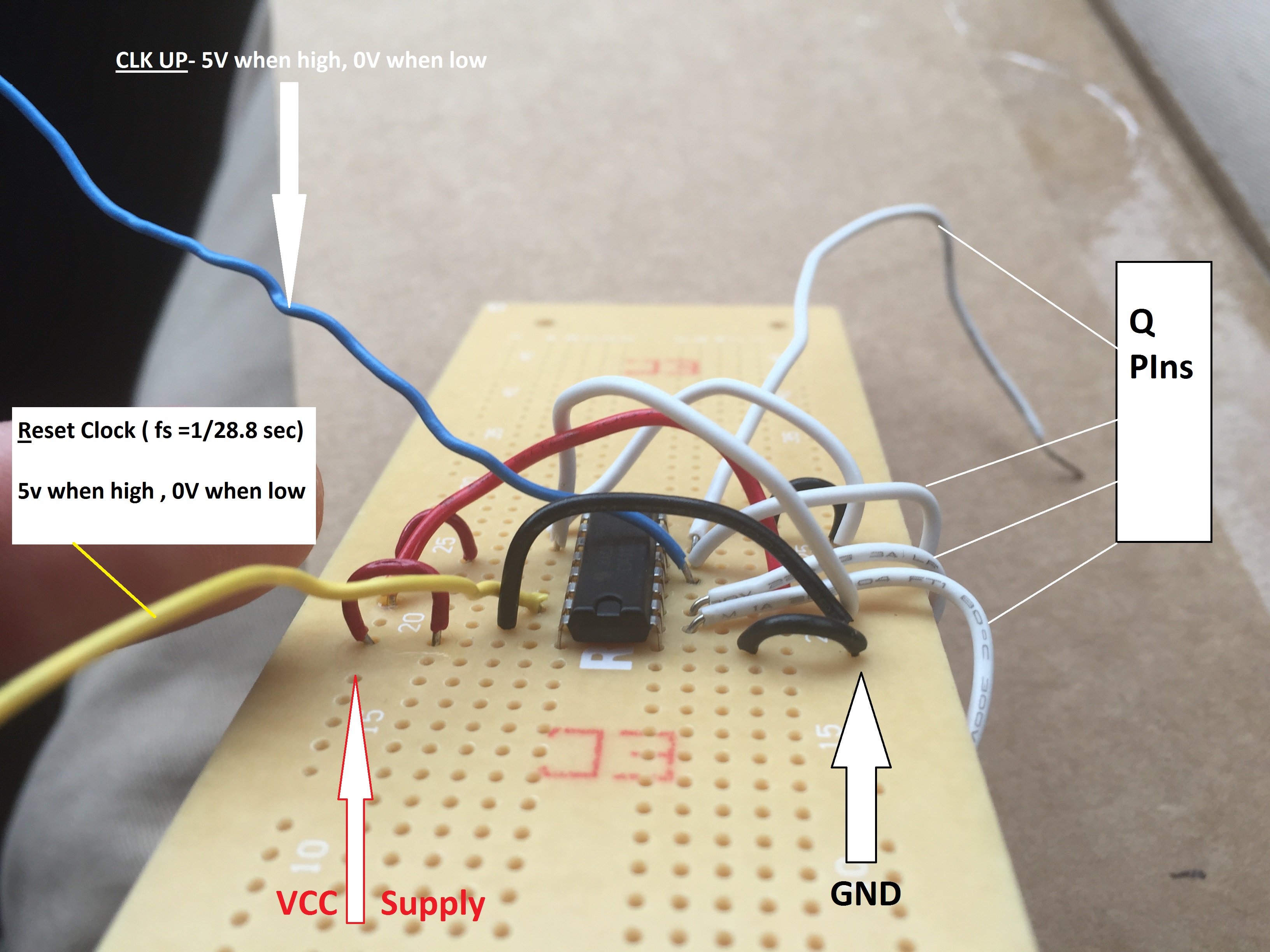
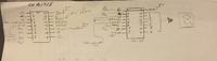
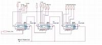
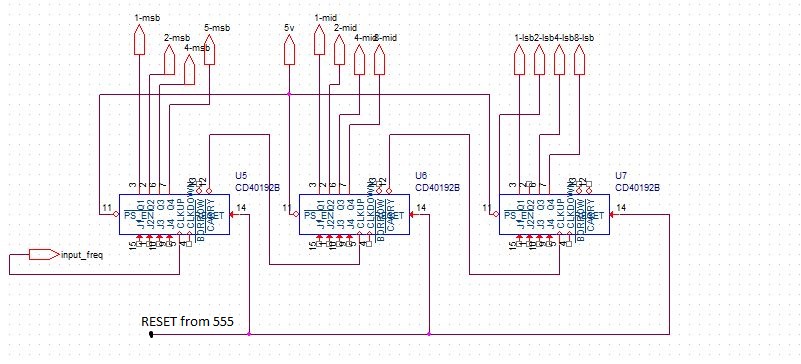
Attached is also a sketch of the connections i have made for the counter please note that this sketch shows the connections for a single set of counter and decoders . I have also shown a connection scheme for the cascaded counters in an additional image


As of now i have built and tested the circuit however the counters don't seem to work properly, when checking them i don't see it counting when probing the Q outputs using an oscilloscope, i only see noise.

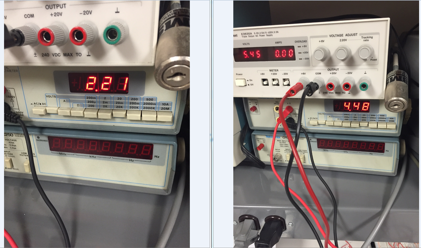
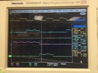
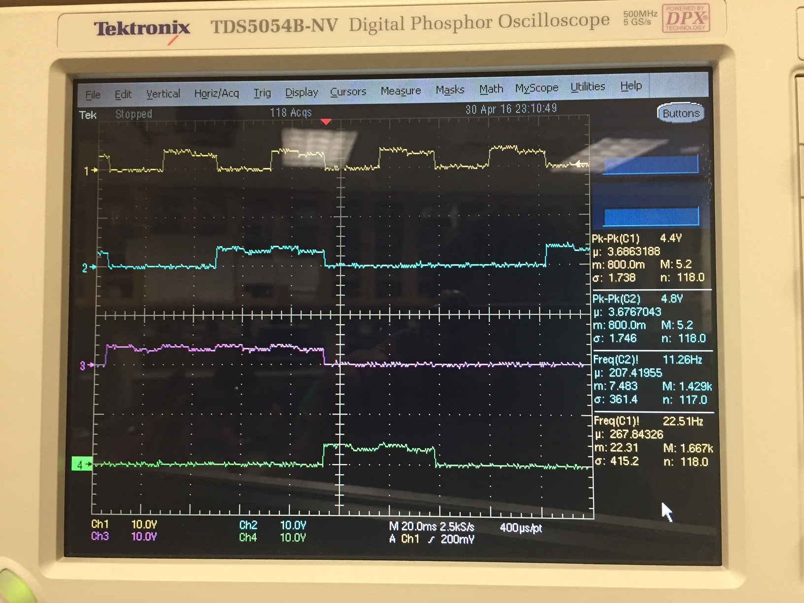
I then built a single counter and decoder to see if maybe something was connected improperly and here i periodically saw a count when using the scope however it was not very clean (Image attached) . Even then the however the decoders did not output anything. When probing the a-g pins on the decoder with a voltmeter i saw the decoder was sending nothing to the 7 segment displays as the voltmeter always read 0V across those pins


Please let me know if any of the connections shown are incorrect i would really appreciate the feedback! I am sure there is something i am forgetting to do which is why the set up is giving me nothing, thank you in advance!

Link to Data Sheets:
https://www.mouser.com/ds/2/405/cd4511b-452627.pdf
https://www.mouser.com/ds/2/405/cd40192b-439702.pdf
 

https://www.edaboard.com?t=353963

Clock Down must be high for it to work. I suggest you also tie the 'J' inputs to ground. It is a CMOS device so no inputs should be left floating.

Note that the 7447 and CD4511 are not directly interchangeable although they do the same job.

Brian.
 

Re: [moved] Frequency Synthesizer using CD4046 PLL / Frequency Multiplication

Clock Down must be high for it to work. I suggest you also tie the 'J' inputs to ground. It is a CMOS device so no inputs should be left floating.

Note that the 7447 and CD4511 are not directly interchangeable although they do the same job.

Brian.

Thanks brian I will try it again with the J inputs to GND

What about the LT, BI/RBO & RBI Pins for the CD4511 ?
 

Re: [moved] Frequency Synthesizer using CD4046 PLL / Frequency Multiplication

The waveforms look very noisy, I suggest you look at the +5v supply and see if that is noisy too. Some suitably large bypass capacitors may help.
 

Re: [moved] Frequency Synthesizer using CD4046 PLL / Frequency Multiplication

What about the LT, BI/RBO & RBI Pins for the CD4511 ?

LT = Lamp Test. Although LEDs are almost always used, the name 'lamp' has stuck for historical reasons. If you pull LT low it turns all the outputs on to check all the 'lamps' are working. For normal use, it should be high all the time.

RBO and RBI = Ripple Blanking Output and Ripple Blanking Input, on the 7447 they can be used to turn all the segments off. This is useful in cases where the display has more than one digit and they have to be multiplexed. On the 4511 the function (BI) is slightly different, it works as an output enable control, if you drive BI low it turns all the segments off so normally you should tie it high. You can pulse it rapidly to control the brightness using a PWM signal.

LE (on the 4511) is the Latch Enable, it allows you to freeze the segment output pattern when the input signal is still changing. You use it when you share the data inputs in parallel with other 4511 devices to route it to one specific IC. Normally you keep it tied low so the number on the data inputs is immediately shown on the LED but if you lift the pin to logic high, whatever was on the data pins at the time it went from 0 to 1 is frozen on the display.

Brian.
 

Re: [moved] Frequency Synthesizer using CD4046 PLL / Frequency Multiplication

LT = Lamp Test. Although LEDs are almost always used, the name 'lamp' has stuck for historical reasons. If you pull LT low it turns all the outputs on to check all the 'lamps' are working. For normal use, it should be high all the time.

RBO and RBI = Ripple Blanking Output and Ripple Blanking Input, on the 7447 they can be used to turn all the segments off. This is useful in cases where the display has more than one digit and they have to be multiplexed. On the 4511 the function (BI) is slightly different, it works as an output enable control, if you drive BI low it turns all the segments off so normally you should tie it high. You can pulse it rapidly to control the brightness using a PWM signal.

LE (on the 4511) is the Latch Enable, it allows you to freeze the segment output pattern when the input signal is still changing. You use it when you share the data inputs in parallel with other 4511 devices to route it to one specific IC. Normally you keep it tied low so the number on the data inputs is immediately shown on the LED but if you lift the pin to logic high, whatever was on the data pins at the time it went from 0 to 1 is frozen on the display.

Brian.

Thank you for explaining and pointing that out! I built a regular counter with the configuration you described and it seems to be working! If you would have not explained the purpose of each pin i would have not realized these mistakes. Now its time to cascade the counters and see if we can build this counter

Before i do let me ask you the following, if im going to Tie LT, BL High do i need the 1k resistor connected to VCC or can i apply VCC directly to these pins?
 

You probably need to resort to testing the devices individually. Start with the 7-segment display, and build backwards. Verify that all led's light. Confirm which is the direction of current for proper operation.

Add the 7447 and resistors. Pull pins low or high as necessary. Leave no input pin unconnected (floating).

Etc.

The noise on your scope traces looks like it might result from sudden changes in current draw by IC's. Does the power supply have similar spikey waveforms?

The family of TTL IC's (7400 series) are known for drawing sudden strong current spikes. Guidelines recommend putting a .1 uF capacitor across supply pins.

- - - Updated - - -

Update:

Now I see your post in your other thread, saying that you got this to work.
 

It was working for a small amount of time but have the following issue:

Initially the MSB counted from 0-9 and reset periodically as if the counter was not working properly . When looking at the q pins the counter seemed to be counting just fine.

Shortly after I turned off the voltage supplies and input pulses to check wiring. After powering back up I saw all displays show zero no matter what the reset or the clock up was , even if I turned them off

I have done the following for each counter:

Clock up - input frequecny we want to count

Reset- 28.8 sec clock

Clock down- held high

Preset enable- held high

J pins held to gnd

Now for the 4511

Bi-high
Lamp-high
Le-low

A-Q1
B-Q2
C-Q3
D-Q4


When I check the q pins now I see the counter is no longer counting . There is only noise at each pin and I can't seem to understand what I'm doing wrong
 

Re: [moved] Frequency Synthesizer using CD4046 PLL / Frequency Multiplication

The pins are voltage level sensitive and draw virtually no current so it is up to you whether you connect them directly to VCC or use a resistor. The current that would flow through it is so small that even a much higher value resistor could be used if you wanted one. For low cost, you can just connect to VCC but some people would argue that if you did that you lose the ability to pull the pin low (example = for debugging) without shorting out the supply. The choice is really yours, it makes no difference to operation but you must never leave a CMOS input disconnected, because the current they draw is so tiny that there isn't enough to discharge interference pick up on the pin and they could adopt any logic level.

From your description the two ICs seem to be wired correctly. The reset signal should make the output go to '0' and stay there until reset goes low again. If the count intermittently resets by itself, either there is some interference on the reset signal or the power lines are dipping enough to fool the counters into resetting themselves. You should have a capacitor of 100nF directly across the VCC and GND pins of each IC and they should be fitted as close as possible across the IC pins. Also ensure your supply is able to deliver the LED current which varies according to how many segments are lit. For example, if you pass 10mA per segment the current will vary between nothing if all segments are off to about 80mA when they are all on, that is more than a small battery might be able to manage, especially if you have (you should have!) a regulator in the supply to stabilize the 5V.

Brian.

I will try to build this again with the additional 0.1uF caps you suggested and see if this is whats giving me trouble

Now you also mentioned no pins should be left open on CMOS devices due to there current draw which leads the problems you described. When you mentioned this i realized that the Borrow pin on all 40192B devices and the carry pin on the third counter being cascaded are all open. Could this potentially cause problems?

**broken link removed**

**broken link removed**
 
Last edited:

The borrow and carry pins are outputs, so there will be no problem leaving them disconnected.

One further thought. Its not that difficult to damage these CMOS ICs through electrostatic discharge through careless handling.
If they have been "zapped" they can then either misbehave or fail totally.
Always good to have a few extra spares ready stored in conductive foam.


Thank you for confirming i can leave those pins open. DO you know if there a simple test i can conduct to determine if i might have damaged the devices?
 

The simple test is if it works or not.

If it was working and stops, and all the connections appear to be o//k, and if it works again after replacing the chip, chances are the chip has blown.
 

Additional attempts have been made to rebuild a single counter however i find the following issues:

When building it on a breadboard:

Oscilloscope picks up nothing but noise on all Q pins, and very rarely you see a pulse form on Q1, however on average 0V are seen on all Q pins

I checked the VCC pin with a voltmeter and saw something quite odd. When powering up the DC supply i read approximately 4.52 V even though 5.45V were supplied by the source and seconds after the VCC pin drops to 2.4V. (See Image attached)


Protoboard:

With this i decided maybe something was going on with the breadboard so i decided to build and solder a single counter on a protoboard. When doing the oscilloscope still read nothing across the Q pins however in this case when using the voltmeter the 5.45V applied was present at the VCC pin. After letting it run the voltage across VCC pin did not drop as in the bread board case

I dont know why its not working anymore, even after building with new parts i get the same issue. This is quite puzzling because not too long ago i had at least one counter functioning


Just to ensure im not making a connection mistake would someone be so kind to summarize the connections i should be making for the counters and decoders?


I checked the VCC pin with a voltmeter and saw something quite odd. When powering up the DC supply i read approximately 4.52 V even though 5.45V
That sounds like the connection to the 5.45v supply is completely open circuit.
What you are measuring as 4.52v could be coming from the signal generator providing the clocking input, via the static protection diodes within the chip.
Its a fairly common occurrence with "rats nest" quickie prototypes.

I have done the following for each counter:

Clock up - input frequecny we want to count

Reset- 28.8 sec clock

Clock down- held high

Preset enable- held high

J pins held to gnd

Now for the 4511

Bi-high
Lamp-high
Le-low

A-Q1
B-Q2
C-Q3
D-Q4
First thing to confirm is that you are using a 40192 and not a 4192.
Both are presetable decade up down counters that have almost identical functions, but the pin outs are just slightly different enough to cause some real confusion.
 

CMOS devices are prone to damage if you reverse the polarity betwen the pins. The voltages must never go below VSS (which would mean negative with respect to ground in your case) or higher then VDD. Possibly by not connecting VDD you have broken that rule because VDD was lower than the signal you were counting and possibly the other 'pulled high' pins. However, in my experience, when a CMOS logic gate is damaged that way it tends to draw a lot of current and that would be noticed on your power supply display. I would guess the current drawn by the counter stage would be less than 0.1mA so it wouldn't normally show on the PSU. The 7-segment decoder would draw considerably more and the amount would be the sum of all lit segment currents.

If the ICs are still good, it has to be a problem with your wiring I'm afraid, the connections all seem to be to the right places. Can you post a photograph of the construction please.

Brian.


Attached a detailed image along with a PDF document with more images to help put things in perspective, thank you for helping me troubleshoot this by the way!

View attachment Counter.pdf
 

Oh I'm sorry i should have mentioned that 7447 was just a sample image I posted to show how I assumed the 4511 chip I was using would have to be connected


However right now I'm attempting to build a single counter alone , I figured it be easier to trouble shoot the input stage first since I saw he counters were no longer functioning properly

Once I can resolve the issue with the counters I can then add the decoder/ displays
 

From the photograph, I would be surprised if it DID work!

You absolutely MUST connect a decoupling capacitor across VSS and VDD. The reason is that although CMOS ICs draw very little current when in a fixed logic state, they do draw a 'spike' of current as the logic levels change. It is caused by the internal capacitance of the transistors having to be discharged and recharged as the voltage on them changes to the other level. Even the tiny inductance of the wires to the supply, and deficiencies in the supply itself will cause a drop in voltage by the time it reaches the VSS and VDD pins. The drop will be very short, maybe only nanoseconds long but it can be long enough to upset the internal circuits of the IC. Placing a capacitor very close across VSS and VDD gives it a reserve of power exactly where it is needed and help to preven the dip in voltage.

Brian.
 

Status
Not open for further replies.

Part and Inventory Search

Welcome to EDABoard.com

Sponsor

Back
Top